54ACT109
54ACT109 is Dual JK Positive Edge-Triggered Flip-Flop manufactured by National Semiconductor.
- Part of the 54AC109 comparator family.
- Part of the 54AC109 comparator family.
Description
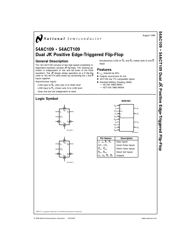
The ’AC/’ACT109 consists of two high-speed pletely independent transition clocked JK flip-flops. The clocking operation is independent of rise and fall times of the clock waveform. The JK design allows operation as a D flip-flop (refer to ’AC/’ACT74 data sheet) by connecting the J and K inputs together. Asynchronous Inputs: LOW input to SD (Set) sets Q to HIGH level LOW input to CD (Clear) sets Q to LOW level Clear and Set are independent of clock Simultaneous LOW on CD and SD makes both Q and Q HIGH
Features n n n n ICC reduced by 50% Outputs source/sink 24 m A ’ACT109 has TTL-patible inputs Standard Military Drawing (SMD)
- ’AC109: 5962-89551
- ’ACT109: 5962-88534
Logic Symbol
IEEE/IEC
DS100267-1 DS100267-7
Pin Names J1, J2, K1, K2 CP1, CP2 CD1, CD2 SD1, SD2 Q1, Q2, Q1, Q2
DS100267-2
Description
Data Inputs Clock Pulse Inputs Direct Clear Inputs Direct Set Inputs Outputs
FACT ® is a registered trademark of Fairchild Semiconductor Corporation.
© 1998 National Semiconductor Corporation
DS100267
.national.
Connection Diagrams
Pin Assignment for DIP and Flatpak Pin Assignment for LCC
DS100267-3 DS100267-4
Truth Table
(each half) Inputs SD L H L H H H H H CD H L L H H H H H CP X X X
Outputs J X X X L H L H X K X X X L L H H X H Q0 Q H L H L Toggle Q0 Q0 L Q0 Q L H H H
H = HIGH Voltage Level L = LOW Voltage Level N = LOW-to-HIGH Transition X = Immaterial Q0(Q0) = Previous Q0 (Q0) before LOW-to-HIGH Transition of Clock
Logic Diagram
(one half shown)
DS100267-5
Please note that this diagram is provided only for the understanding of logic operations and should not be used to estimate propagation delays.
.national.
Absolute Maximum Ratings (Note 1)
If Military/Aerospace specified devices are required, please contact the National Semiconductor Sales Office/ Distributors for availability and specifications. Supply Voltage (VCC) DC Input Diode Current (IIK) VI =
- 0.5V VI = VCC + 0.5V DC Input Voltage (VI) DC Output Diode Current...