54FCT540
54FCT540 is Octal Buffer/Line Driver manufactured by National Semiconductor.
Description
The ’FCT540 is an octal buffer/line drivers designed to be employed as memory and address drivers, clock drivers and bus oriented transmitter/receivers.
These devices are similar in function to the ’FCT240 while providing flow-through architecture (inputs on opposite side from outputs). This pinout arrangement makes these devices especially useful as output ports for microprocessors, allowing ease of layout and greater PC board density.
Features n TRI-STATE inverting outputs n Inputs and outputs opposite side of package, allowing easier interface to microprocessors n TTL input and output level patible n CMOS power consumption n Output sink capability of 48m A, source capability of 12 m A n Standard Microcircuit Drawing (SMD) 5962-8976701
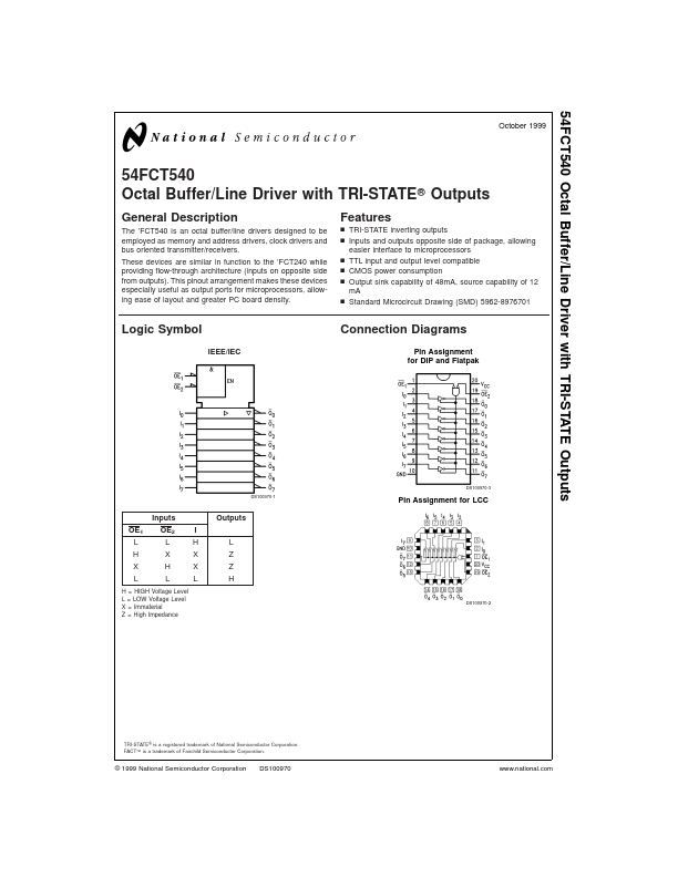
Logic Symbol
IEEE/IEC
Connection Diagrams
Pin Assignment for DIP and Flatpak
Inputs
OE1 L
OE2 L
H XX
X HX
L LL
H = HIGH Voltage Level L = LOW Voltage Level X = Immaterial Z = High Impedance
DS100970-1
Outputs
DS100970-3
Pin Assignment for LCC
DS100970-2
TRI-STATE® is a registered trademark of National Semiconductor Corporation. FACT™ is a trademark of Fairchild Semiconductor Corporation.
© 1999 National Semiconductor Corporation DS100970
.national.
Absolute Maximum Ratings (Note 1)
If Military/Aerospace specified devices are required, please contact the National Semiconductor Sales Office/ Distributors for availability and specifications.
Supply Voltage (VCC) DC Input Diode Current (IIK)
VI =
- 0.5V VI = VCC + 0.5V DC Input Voltage (VI) DC Output Diode Current (IOK) VO =
- 0.5V VO = VCC + 0.5V DC Output Voltage (VO) DC Output Source or Sink Current (IO) DC VCC or Ground Current per Output Pin (ICC or IGND)
- 0.5V to +7.0V
- 20 m A +20 m A
- 0.5V to VCC + 0.5V
- 20 m A +20 m A
- 0.5V to VCC + 0.5V
±50 m A
±50 m A
Storage Temperature (TSTG) Junction Temperature...