54LS174
54LS174 is Hex/Quad D Flip-Flops manufactured by National Semiconductor.
Description
These positive-edge-triggered flip-flops utilize TTL circuitry to implement D-type flip-flop logic All have a direct clear input and the quad (175) versions feature plementary outputs from each flip-flop
Information at the D inputs meeting the setup time requirements is transferred to the Q outputs on the positive-going edge of the clock pulse Clock triggering occurs at a particular voltage level and is not directly related to the transition time of the positive-going pulse When the clock input is at either the high or low level the D input signal has no effect at the output
Features
Y LS174 contains six flip-flops with single-rail outputs Y LS175 contains four flip-flops with double-rail outputs Y Buffered clock and direct clear inputs Y Individual data input to each flip-flop Y Applications include
Buffer storage registers Shift registers Pattern generators Y Typical clock frequency 40 MHz Y Typical power dissipation per flip-flop 14 m W Y Alternate Military Aerospace device (54LS174 54LS175) is available Contact a National Semiconductor Sales Office Distributor for specifications
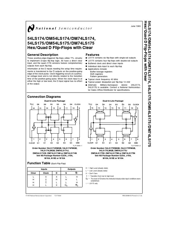
Connection Diagrams
Dual-In-Line Package
Dual-In-Line Package
TL F 6404
- 1
Order Number 54LS174DMQB 54LS174FMQB 54LS174LMQB DM54LS174J
DM54LS174W DM74LS174M or DM74LS174N See NS Package Number E20A J16A M16A N16E or W16A
TL F 6404
- 2
Order Number 54LS175DMQB 54LS175FMQB 54LS175LMQB DM54LS175J
DM54LS175W DM74LS175M or DM74LS175N See NS Package Number E20A J16A M16A N16E or W16A
Function Table (Each Flip-Flop)
Clear
Inputs
Clock
X u u
Outputs
LH HL LH Q0 Q0
H e High Level (steady state)
L e Low Level (steady state)
X e Don’t Care u e Transition from low to high level
Q0 e The level of Q before the indicated steady-state input conditions were established e LS175 only
C1995 National Semiconductor Corporation TL F 6404
RRD-B30M105 Printed in U S A
Absolute Maximum Ratings (Note)
If Military Aerospace specified devices are required please...