ADC1021
ADC1021 is 10-Bit uP Compatible A/D Converter manufactured by National Semiconductor.
Description
The ADC100l and ADC1021 are CMOS, 10-bit successive
- Easily interlaced to 6800 ,..p derivatives with minimal approximation AID converters. The 20-pin ADC100l is pin external logic patible with the ADC0801 8-bit AID family. The 10-bit data word is read in two 8-bit bytes, formatted left justified and high byte first. The six least significant bits of the second byte are set to zero, as is proper for a 16-bit word.
The 24-pin ADC1021 outputs 10 bits parallel and is intended for interlace to a 16-bit data bus.
Differential inputs provide low frequency input mon
- Differential analog voltage inputs
- Logic inputs and outputs meet both MOS and TTL volt- age level specifications
- Works with 2.5V (LM336) voltage reference
- On-chip clock generator
- OV to 5V analog input voltage range with single 5V sup- ply mode rejection and allow offsetting the analog range of the converter. In addition, the reference input can be adjusted enabling the conversion of reduced analog ranges with 10bit resolution.
- Operates ratiometrically or with 5 Voc, 2.5 Voc, or analog span adjusted voltage reference
- 0.3" standard width 20-pin DIP package or 24 pins with 1O-bit parallel output
Features
- ADC100l is pin patible with ADC0801 series 8-bit AID converters
- patible with NSC800 and 8080 ,..p derivatives-no interlacing logic needed
Key Specifications
- Resolution
- Linearity error
- Conversion time
10 bits ±1 LSB
200,..S
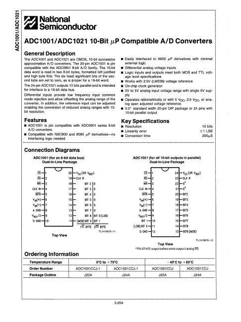
Connection Diagrams
ADC100l (for an 8-bit data bus) Dual-In-Llne Package
ADC102l (for alll0- bit outputs in parallel) Dual- ln- Line Package
CS-l
Rii- 2
..../
20 I-Vcc(OR VREF) 191-Cl K R i VR-3 Cl K IN- 4
181171-
BIT 2 0 BIT 3 0
INTR- 5 VIN(+)- 6 VIN(-)- 7 A GND- 8 VREF/2- 9 D GND- 10
161-
BIT 4 0
151-
BIT 5 0
141-
BIT 6 0
131-
BIT 7 0
12J- a IT 8 a IT O(LSB) ll J-(Ioi SB)BIT 9 BIT...