CD4027BM
CD4027BM is Dual J-K Master/Slave Flip-Flop manufactured by National Semiconductor.
Description
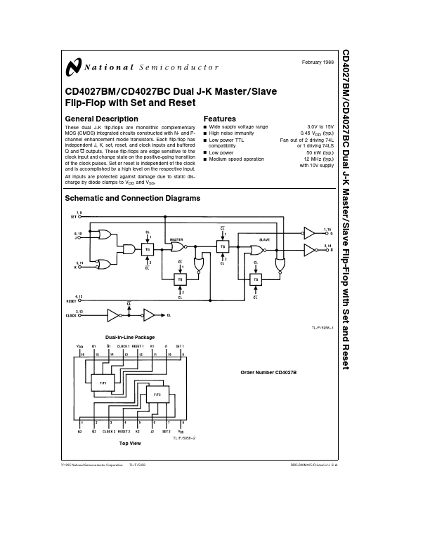
These dual J-K flip-flops are monolithic plementary MOS (CMOS) integrated circuits constructed with N- and Pchannel enhancement mode transistors Each flip-flop has independent J K set reset and clock inputs and buffered Q and Q outputs These flip-flops are edge sensitive to the clock input and change state on the positive-going transition of the clock pulses Set or reset is independent of the clock and is acplished by a high level on the respective input All inputs are protected against damage due to static discharge by diode clamps to VDD and VSS
Features
Wide supply voltage range High noise immunity Low power TTL patibility Low power Medium speed operation
3 0V to 15V 0 45 VDD (typ ) Fan out of 2 driving 74L or 1 driving 74LS 50 n W (typ ) 12 MHz (typ ) with 10V supply
Schematic and Connection Diagrams
TL F 5958
- 1
Dual-In-Line Package
Order Number CD4027B
TL F 5958
- 2
Top View
C1995 National Semiconductor Corporation
TL F 5958
RRD-B30M105 Printed in U S A
Absolute Maximum Ratings
(Note 1 and 2)
If Military Aerospace specified devices are required please contact the National Semiconductor Sales Office Distributors for availability and specifications b 0 5 VDC to a 18 VDC DC Supply Voltage (VDD) b 0 5V to VDD a 0 5 VDC Input Voltage (VIN) b 65 C to a 150 C Storage Temperature Range (TS) Power Dissipation (PD) Dual-In-Line 700 m W Small Outline 500 m W Lead Temperature (TL) (Soldering 10 seconds) 260 C
Remended Operating Conditions (Note 2)
DC Supply Voltage (VDD) Input Voltage (VIN) Operating Temperature Range (TA) CD4027BM CD4027BC 3V to 15 VDC 0V to VDD VDC b 55 C to a 125 C b 40 C to a 85 C
DC Electrical Characteristics CD4027BM (Note 2)
Symbol IDD Parameter Conditions b 55 C a 25 C a 125 C
Units m A m A m A V V V V V V
Min Quiescent Device Current VDD e 5V VIN e VDD or VSS VDD e 10V VIN e VDD or VSS VDD e 15V VIN e VDD or VSS Low Level Output Voltage
Max 1 2 4 0 05 0 05 0 05
Min
Typ
Max 1 2 4
Min
Max 30 60 120 0 05 0...