CD4027BMS
Overview
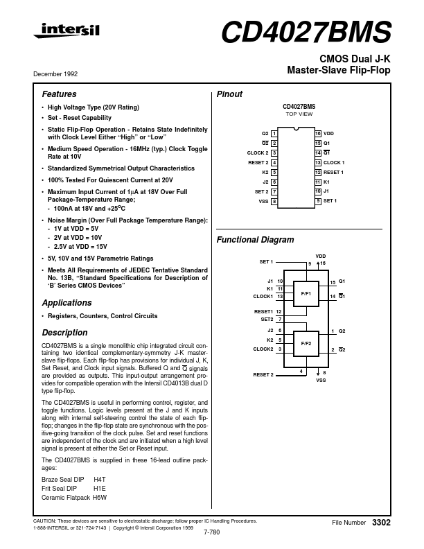
CD4027BMS is a single monolithic chip integrated circuit containing two identical complementary-symmetry J-K masterslave flip-flops. Each flip-flop has provisions for individual J, K, Set Reset, and Clock input signals.
- High Voltage Type (20V Rating)
- Set - Reset Capability
- Static Flip-Flop Operation - Retains State Indefinitely with Clock Level Either “High” or “Low”
- Medium Speed Operation - 16MHz (typ.) Clock Toggle Rate at 10V
- Standardized Symmetrical Output Characteristics
- 100% Tested For Quiescent Current at 20V
- Maximum Input Current of 1µA at 18V Over Full Package-Temperature Range; - 100nA at 18V and +25oC
- Noise Margin (Over Full Package Temperature Range): - 1V at VDD = 5V - 2V at VDD = 10V - 2.5V at VDD = 15V
- 5V, 10V and 15V Parametric Ratings
- Meets All Requirements of JEDEC Tentative Standard No. 13B, “Standard Specifications for Description of ‘B’ Series CMOS Devices”