CGS64B2529
CGS64B2529 is 1 to 10 Minimum Skew Clock Driver manufactured by National Semiconductor.
- Part of the CGS6482529 comparator family.
- Part of the CGS6482529 comparator family.
Description
This minimum skew clock driver is designed for Clock Gen- eration and Support (CGS) applications operating from 33 MHz to 80 MHz. The devices guarantee minimum output skew across the outputs of a given device.
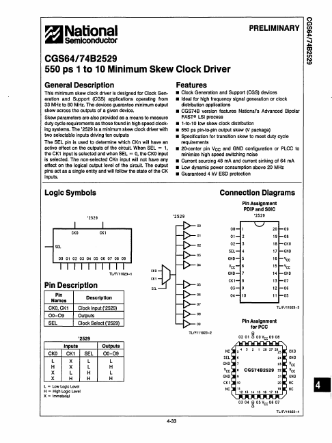
Skew parameters are also provided as a means to measure duty cycle requirements as those found in high speed clock- ing systems. The '2529 is a minimum skew clock driver with two selectable inputs driving ten outputs
The SEL pin is used to determine which CKn will have an active effect on the outputs of the circuit. When SEL = 1, the CK1 input is selected and when SEL = 0, the CKO input is selected. The non-selected CKn input will not have any effect on the logical output level of the circuit The output pins act as a single entity and will follow the state of the CK inputs.
Features
- Clock Generation and Support (CGS) devices
- Ideal for high frequency signal generation or clock distribution applications
- CGS74B version features
National's Advanced Bipolar
FAST«I LSI process
- 1- to-10 low skew clock distribution
- 550 ps pin-to-pin output skew CV package)
- Specification for transition skew to meet duty cycle requirements
- 20-center pin Vee and GND configuration or PLCC to minimize high speed switching noise
- Current sourcing 48 rn A and current sinking of 64 m A
- Low dynami C power consumption above 20 MHz
- Guaranteed 4 k V ESD protection
Logic Symbols
'2529
SEL 00 01 02 03 0.. 05 06 07 08 09
TLl F/11923-1
Pin Description
Pin Names CKO,CK1 00-09 SEL
Description
Clock Input (,2529) Outputs Clock Select (,2529)
'2529
Inputs
CKO CK1...