CGS64CT801
CGS64CT801 is Low Skew PLL 1-to-8 CMOS Clock Driver manufactured by National Semiconductor.
- Part of the CGS64C800 comparator family.
- Part of the CGS64C800 comparator family.
Description
,!')
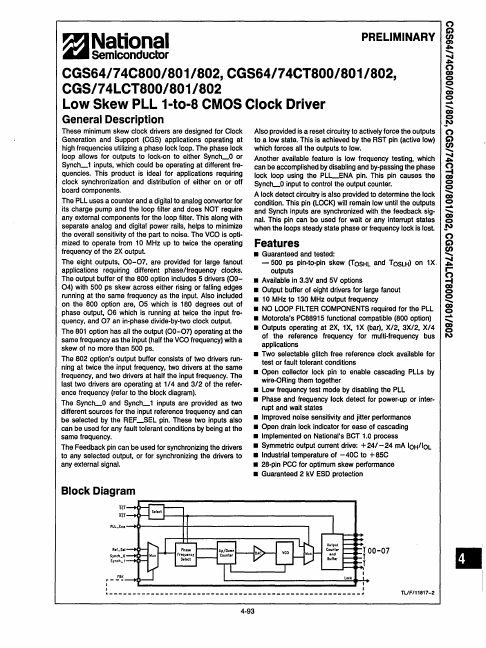
These minimum skew clock drivers are designed for Clock Generation and Support (CGS) applications operating at high frequencies utilizing a phase lock loop. The phase lock loop allows for outputs to lock-on to either Sync LO or Sync L1 inputs, which could be operating at different frequencies. This product is ideal for applications requiring clock synchronization and distribution of either on or off board ponents.
The PLL uses a counter and a digital to analog convertor for its charge pump and the loop filter and does NOT require any external ponents for the loop filter. This along with separate analog and digital power rails, helps to minimize the overall sensitivity of the part to noise. The VCO is optimized to operate from 10 MHz up to twice the operating frequency of the 2X output.
The eight outputs, 00-07, are provided for large fanout applications requiring different phase/frequency clocks. The output buffer of the SOO option includes 5 drivers (0004) with 500 ps skew across either rising or falling edges running at the same frequency as the input. Also included on the SOO option are, 05 which is 1S0 degrees out of phase output, 06 which is running at twice the input frequency, and 07 an in-phase divide-by-two clock output.
The S01 option has all the output (00-07) operating at the same frequency as the input (half the VCO frequency) with a skew of no more than 500 ps.
The S02 option's output buffer consists of two drivers running at twice the input frequency, two drivers at the same frequency, and two drivers at half the input frequency. The last two drivers are operating at 1/4 and 3/2 of the reference frequency (refer to the block diagram).
The Sync LO and Synch_1 inputs are provided as two different sources for the input reference frequency and can be selected by the REF_SEL pin. These two inputs also o Also provided is a reset circuitry to actively force the outputs to a low state. This is achieved by the RST pin (active low) which...