CGS74B2525
CGS74B2525 is 1-to-8 Minimum Skew Clock Driver manufactured by National Semiconductor.
Description
This minimum skew clock driver is designed for Clock Generation and Support (CGS) applications operating well above 20 MHz (33 MHz 50 MHz) The device guarantees minimum output skew across the outputs of a given device and also from device-to-device Skew parameters are also provided as a means to measure duty cycle requirements as those found in high speed clocking systems The ’B2525 is a minimum skew clock driver with one input driving eight outputs specifically designed for signal generation and clock distribution applications
Features
Clock Generation and Support (CGS) Device Ideal for high frequency signal generation or clock distribution applications CGS74B version features
National’s Advanced Bipolar FAST LSI process 1-to-8 low skew clock distribution 600 ps pin-to-pin output skew Specifications for device-to-device variation of propagation delay Specification for transition skew to meet duty cycle requirements Center pin VCC and GND configuration to minimize high speed switching noise Current sourcing 48 m A and current sinking of 64 m A Low dynamic power consumption above 20 MHz Guaranteed 4 k V ESD protection
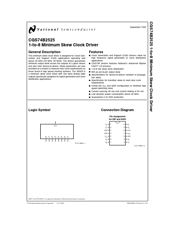
Logic Symbol
Connection Diagram
Pin Assignment for DIP and SOIC
TL F 10907
- 1 TL F 10907
- 2
FAST and TRI-STATE are registered trademarks of National Semiconductor Corporation C1995 National Semiconductor Corporation TL F 10907 RRD-B30M115 Printed in U S A
Functional Description
Pin Description
Pin Names CLK O0
- O7 Description
Clock Input Outputs
Truth Table
Inputs CLK L H Outputs O0
- O7 L H
TL F 10907
- 5
Absolute Maximum Ratings (Note 1)
If Military Aerospace specified devices are required please contact the National Semiconductor Sales Office Distributors for availability and specifications Supply Voltage (VCC) Input Voltage (VI) Operating Free Air Temperature Storage Temperature Range Junction Temperature (i JA) Plastic (N) Package JEDEC SOIC (M) Package 7 0V 7 0V 0 C to a 70 C b 65 C to a 150 C 104...