CGS74CT2524
CGS74CT2524 is 1 to 4 Minimum Skew (300 ps) Clock Driver manufactured by National Semiconductor.
Description
These minimum skew clock drivers are designed for Clock Generation and Support (CGS) applications operating at high frequencies This device guarantees minimum output skew across the outputs of a given device Skew parameters are also provided as a means to measure duty cycle requirements as those found in high speed clocking systems The CGS74CT2524 is a minimum skew clock driver with one input driving four outputs specifically designed for signal generation and clock distribution applications
Features
Y Y Y Y Y Y Y Y
Guaranteed 300 ps pin-to-pin skew (t OSHL and t OSLH) Implemented on National’s FACTTM family process 1 input to 4 outputs low skew clock distribution Symmetric output current drive 24 m A IOH IOL Industrial temperature of b40 C to a 85 C 8-pin SOIC package Low dynamic power consumption above 20 MHz Guaranteed 2 k V ESD protection
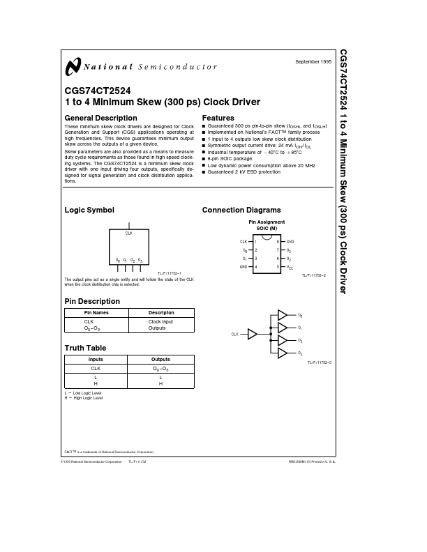
Logic Symbol
Connection Diagrams
Pin Assignment SOIC (M)
TL F 11752- 1
TL F 11752
- 2
The output pins act as a single entity and will follow the state of the CLK when the clock distribution chip is selected
Pin Description
Pin Names CLK O0
- O3 Descripton Clock Input Outputs
Truth Table
Inputs CLK L H
L e Low Logic Level H e High Logic Level
Outputs O0
- O3 L H
TL F 11752
- 3
FACTTM is a trademark of National Semiconductor Corporation C1995 National Semiconductor Corporation TL F 11752 RRD-B30M115 Printed in U S A
Absolute Maximum Ratings (Note)
If Military Aerospace specified devices are required please contact the National Semiconductor Sales Office Distributors for availability and specifications b 0 5 to 7 0V Supply Voltage (VCC) DC Input Voltage Diode Current (IIK) b 20 m A V e b0 5V a 20 m A V e VCC a 0 5V b 0 5V to (VCC a 0 5V) DC Input Voltage (VI) DC Output Diode (Current) (IO) b 20 m A V e b0 5V a 20 m A V e VCC a 0 5V b 0 5V to (VCC a 0 5V) DC Output Voltage (VO) DC Output Source g 50 m A or Sink Current (IO) DC VCC or Ground Current g 50 m A per Output Pin (ICC or IGND) b 65 C to a 150 C Storage...