CLC502
CLC502 is Clamping/ Low-Gain Op Amp with Fast 14-bit Settling manufactured by National Semiconductor.
Description
Features s s s s
Output clamping with fast recovery 0.0025% settling in 25ns (32ns max.) Low power, 170m W Low distortion. -50d Bc at 20MHz Output clamping applications High-accuracy A/D systems (12-14 bits) High-accuracy D/A converters Pulse amplitude modulation systems
Applications s s s s
The CLC502 is available in several versions to meet a variety of requirements. A three-letter suffix determines the version:
CLC502AJP -40°C to +85°C CLC502AJE -40°C to +85°C DESC SMD number: 5962-91743 8-pin plastic DIP 8-pin plastic SOIC
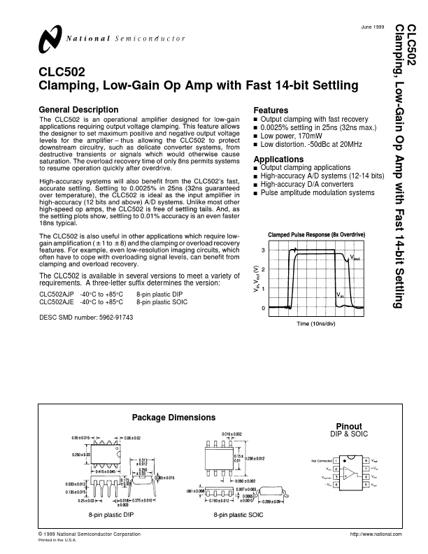
Package Dimensions Pinout
DIP & SOIC
© 1999 National Semiconductor Corporation
Printed in the U.S.A. http://.national.
CLC502 Electrical Characteristics (Av = +2,Vcc = ±5V, RL = 100Ω, Rf = 250Ω,VH = +3V, VL = -3V)
Min/max ratings are based on product characterization and simulation. Individual parameters are tested as noted. Outgoing quality levels are determined from tested parameters.
Absolute Maximum Ratings
Miscellaneous Ratings http://.national.
Typical Performance Characteristics (TA = 25°, Av = +2, VCC = ±5V, RL = 100Ω,
Non-Inverting Frequency Response
Vout = 0.5Vpp Av = 2 Rf = 249Ω Av = 1 Rf = 301Ω
Rf = 250Ω, VH = +3V, VL = -3V )
Inverting Frequency Response
Vout = 0.5Vpp Av = -2 Rf = 237Ω Av = -1 Rf = 249Ω
Phase (deg)
Magnitude (1d B/div)
Magnitude (1d B/div)
0 -90
Av = 8 Rf = 110Ω Av = 4 Rf = 200Ω
-180 -270 -360 -450 100
Phase (deg)
-180 -270
Av = -8 Rf = 210Ω Av = -4 Rf = 249Ω
-360 -450 -540 -630 100
Frequency 10 (MHz)
Frequency 10 (MHz)
3 http://.national. http://.national.
Package Thermal Resistance
Package AJP AJE θJC 65°C/W 60°C/W θJA 120°C/W 140°C/W
Reliability...