CLC503
CLC503 is Comlinear CLC503 180MHz / Differential-Output Amplifier manufactured by National Semiconductor.
Description
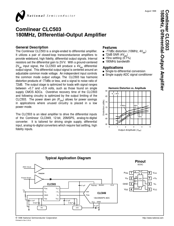
The linear CLC503 is a single-ended to differential amplifier. It utilizes a pair of closed-loop transconductance amplifiers to provide wideband, high fidelity, differential output signals. Internal resistors set the differential gain to 2V/V. With a ground-centered 2Vpp input signal, the CLC503 will produce a 4Vpp differential output signal. This differential output signal is centered around an adjustable mon mode voltage. An independent input controls the mon mode output voltage. The CLC503 has harmonic distortion products of -77d Bc or less, and a signal to noise ratio of 72d B. The output stage is optimized for loads with signal ranges between +0.7 and +3.9 volts, such as those found on single supply CMOS ADCs. Overdrive recovery time of the CLC503 and following circuitry is optimized by the output limiting of the CLC503. The power down pin (PDN) allows for power savings in applications where unused circuitry is placed in a low power mode. The CLC503 is an ideal amplifier to drive the differential inputs of the linear CLC949, 12-bit, 20MSPS, analog-to-digital converter. It is tailored for driving single supply, differential input, analog-to-digital converters which require fast settling, high fidelity inputs.
Features s s s s
-77d Bc distortion (10MHz, 4Vpp) 72d B SNR (4Vpp) 15ns settling (0.1%) 180MHz bandwidth Single-to-differential conversion Single supply ADC signal conditioner
Applications s s
Harmonic Distortion vs. Amplitude
-60
RL = 2kΩ
-65
Distortion (d Bc)
-70
10MHz 5MHz
-75 -80
1MHz
-85 -90 0 1 2
2MHz
Output Amplitude (Vpp)
Typical Application Diagram Pinout
SOIC
ADC Clock
74AC04
PDN Vin
0.1µF Vcm +Vo -Vo VCC 0.1µF 6.8µF +5V VINP VINN VREFMO BIASC CLK
2K AMP 2K CORE
Vcm +Vo -Vo VCC
Power Down
GND VEE
Vin
PDN Vin GND 0.1µF 6.8µF -5V VEE
CLC949
12b/20MSPS ADC
VCC GND
0.1µF
© 1996 National Semiconductor Corporation
Printed in the U.S.A. http://.national.
Electrical Characteristics (VCC = + 5V, VEE =
- 5V,...