CLC522
CLC522 is Wideband Variable-Gain Amplifier manufactured by National Semiconductor.
Description
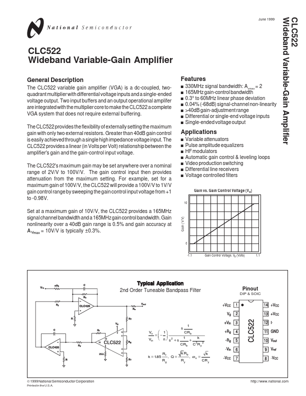
The CLC522 variable gain amplifier (VGA) is a dc-coupled, twoquadrant multiplier with differential voltage inputs and a single-ended voltage output. Two input buffers and an output operational amplifer are integrated with the multiplier core to make the CLC522 a plete VGA system that does not require external buffering. The CLC522 provides the flexibility of externally setting the maximum gain with only two external resistors. Greater than 40d B gain control is easily achieved through a single high impedance voltage input. The CLC522 provides a linear (in Volts per Volt) relationship between the amplifier's gain and the gain-control input voltage. The CLC522's maximum gain may be set anywhere over a nominal range of 2V/V to 100V/V. The gain control input then provides attenuation from the maximum setting. For example, set for a maximum gain of 100V/V, the CLC522 will provide a 100V/V to 1V/V gain control range by sweeping the gain control input voltage from +1 to -0.98V. Set at a maximum gain of 10V/V, the CLC522 provides a 165MHz signal channel bandwidth and a 165MHz gain control bandwidth. Gain nonlinearity over a 40d B gain range is 0.5% and gain accuracy at A Vmax = 10V/V is typically ±0.3%.
Features s s s s s s s
330MHz signal bandwidth: Avmax = 2 165MHz gain-control bandwidth 0.3° to 60MHz linear phase deviation 0.04% (-68d B) signal-channel non-linearity >40d B gain-adjustment range Differential or single-end voltage inputs Single-ended voltage output Variable attenuators Pulse amplitude equalizers HF modulators Automatic gain control & leveling loops Video production switching Differential line receivers Voltage controlled filters
Gain vs. Gain Control Voltage (V g )
Applications s s s s s s s
Gain (V/V)
0 -1.1
Gain Control Voltage, Vg (Volts)
Typical Application 2nd Order Tuneable Bandpass Filter
Pinout
DIP & SOIC
1 = - Vin n s 2 + s Vo Rf Rg s
CRb k 1 + 2 CRb C R y 2 k Rb Ry , ωo = k CR y k = 185 .
, Q=
© 1999...