CLC532
CLC532 is High-Speed 2:1 Analog Multiplexer manufactured by National Semiconductor.
Description
The CLC532 is a high-speed 2:1 multiplexer with active input and output stages. The CLC532 also employs a closed-loop design which dramatically improves accuracy. This monolithic device is constructed using an advanced high-performance bipolar process. The CLC532 has been specifically designed to provide settling times of 17ns to 0.01%. This, coupled with the adjustable noise-bandwidth, makes the CLC532 an ideal choice for infrared and CCD imaging systems. Channel-to-channel isolation is better than 80d B @ 10MHz. Low distortion (80d Bc) and spurious signal levels make the CLC532 a very suitable choice for both I/Q processors and receivers. The CLC532 is offered over both the industrial and military temperature ranges. The Industrial versions, CLC532AJPAJEAID, are specified from -40°C to +85°C and are packaged in 14-pin plastic DIP's, 14-pin SOIC's and 14-pin Side-Brazed packages. The extended temperature versions, CLC532A8B/A8D/A8L-2, are specified from -55°C to +125°C and are packaged in a 14-pin hermetic DIP and 20-terminal LCC packages. (Contact factory for LCC and CERDIP availability.) Ordering Information ...
CLC532AJP CLC532AJE CLC532ALC CLC532AMC CLC532A8B 14-pin plastic DIP 14-pin plastic SOIC dice dice, MIL-STD-833 14-pin CERDIP; MIL-STD-883 20-terminal LCC; CLC532A8L-2A -55o C to +125o C MIL-STD-883 Contact factory for other packages and DESC SMD number. -40o C -40o C -40o C -55o C -55o C to to to to to +85o C +85o C +85o C +125o C +125o C
Features s s s s s
12-bit settling (0.01%)
- 17ns Low noise
- 32µVrms High isolation
- 80d B @ 10MHz Low distortion
- 80d Bc @ 5MHz Adjustable bandwidth
- 190MHz (max) Infrared system multiplexing CCD sensor signals Radar I/Q switching High definition video HDTV Test and calibration
Applications s s s s s
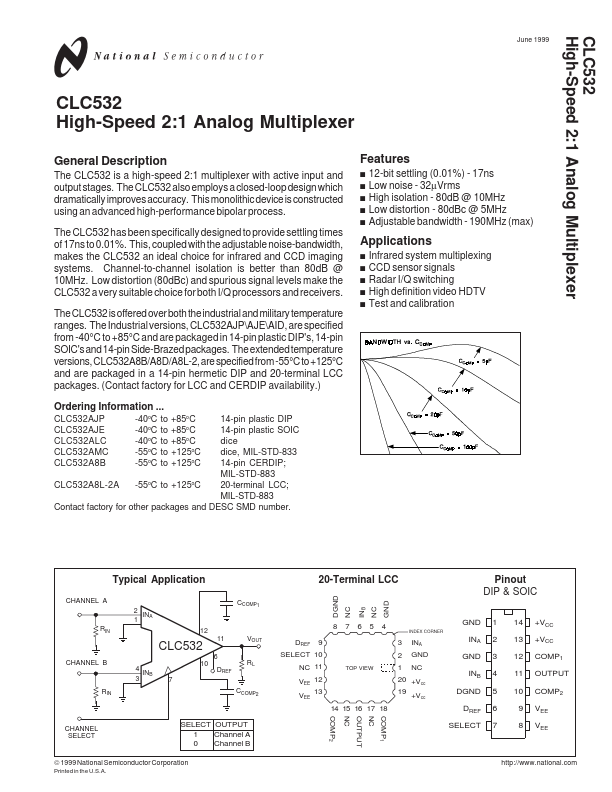
Typical Application
CHANNEL A 2 INA 1 RIN
20-Terminal LCC
GND NC NC INB
CP1
DGND
Pinout DIP & SOIC
INDEX CORNER
11 6 DREF VOUT RL
4 3 2
1 2 3 4 5 6 7
14 13 12 11 10 9 8
+VCC +VCC P1 OUTPUT P2...