CLC5523
CLC5523 is Low-Power/ Variable Gain Amplifier manufactured by National Semiconductor.
Features s s s s s s
Low power: 135m W 250MHz, -3d B bandwidth Slew rate 1800V/ms Gain flatness 0.2d B @ 75MHz Rise & fall times 2.0ns Low input voltage noise 4n V/ÖHz Automatic gain control Voltage controlled filters Automatic signal leveling for A/D Amplitude modulation Variable gain transimpedance
Applications s s s s s
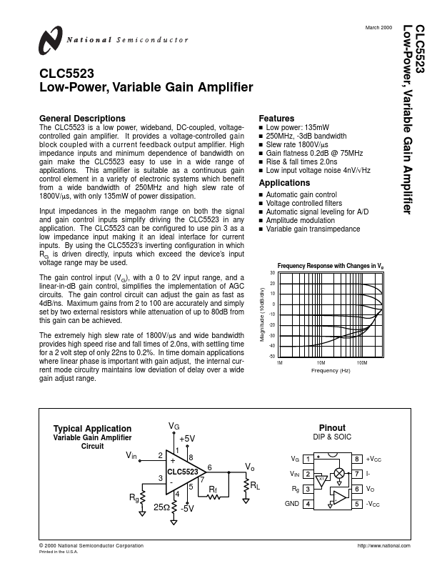
Frequency Response with Changes in Vg
30 20
Magnitude (10d B/div)
10 0 -10 -20 -30 -40 -50 1M 10M 100M
Frequency (Hz)
Typical Application
Variable Gain Amplifier Circuit
VG +5V
2 3 1
Pinout
DIP & SOIC
VG +VCC
X1
+
Vin
+ 4
8 6 7 5
Vo RL
VIN Rg GND
IVO -VCC
Rg
Rf
25W
-5V
© 2000 National Semiconductor Corporation
Printed in the U.S.A. http://.national.
CLC5523 Electrical Characteristics (VCC = ±5V, Rf = 1k, Rg = 100W, RL = 100W, VG = 2V; unless specified)
PARAMETERS Ambient Temperature CONDITIONS CLC5523I TYP +25˚C 250 100 0 0.2 0.6 95 2.0 6.0 22 700 1800 4 -65 -80 -57 -75 5 4 36 50 ±3.8 3.0 3.0 1.0 7.0 7.0 0.04 0.3 0.5 10 1.0 40 57 13.5 ±3.4 ±3.0 0.1 80 146 MIN/MAX RATINGS 25˚C -40 to 85˚C 150 45 0.8 1.0 1.5 70 2.8 15 30 450 1000 125 35 2.0 1.2 3.0 60 3.0 20 60 400 700 UNITS NOTES FREQUENCY DOMAIN RESPONSE -3d B bandwidth Vo < 0.5Vpp Vo < 4.0Vpp peaking DC to 200MHz (Vo = 0.5Vpp) rolloff DC to 75MHz...