DP83241
DP83241 is CDD Device manufactured by National Semiconductor.
Description
The CDD device is a clock generation and distribution device intended for use in FDDI (Fiber Distributed Data Interface) networks The device provides the plete set of clocks required to convert byte wide data to serial format for fiber medium transmission and to move byte wide data between the PLAYERTM and BMACTM devices in various station configurations 12 5 MHz and 125 MHz differential ECL clocks are generated for the conversion of data to serial format and 12 5 MHz and 25 MHz TTL clocks are generated for the byte wide data transfers
Features
Provides 12 5 MHz and 25 MHz TTL clocks 12 5 MHz and 125 MHz ECL clocks 5 phase TTL local byte clocks eliminate clock skew problems in concentrators Internal VCO requires no varactors coils or adjustments Option for use of High Q external VCO 125 MHz clock generated from a 12 5 MHz crystal External PLL synchronizing reference for concentrator configurations 28-pin PLCC package Bi CMOS processing
TL F 10385
- 1
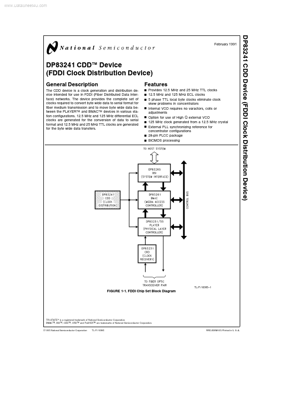
FIGURE 1-1 FDDI Chip Set Block Diagram
TRI-STATE is a registered trademark of National Semiconductor Corporation BMACTM BSITM CDDTM CRDTM and PLAYERTM are trademarks of National Semiconductor Corporation C1995 National Semiconductor Corporation TL F 10385 RRD-B30M105 Printed in U S A
Table of Contents
1 0 FDDI CHIP SET OVERVIEW
2 0 FUNCTIONAL DESCRIPTION
3 0 PIN DESCRIPTIONS 4 0 ELECTRICAL CHARACTERISTICS 4 1 Absolute Maximum Ratings 4 2 Remended Operating Conditions 4 3 DC Electrical Characteristics 4 4 AC Electrical Characteristics 5 0 DETAILED INFORMATION 5 1 External ponents 5 2 Concentrator and Dual Attach Station Configurations 5 3 Layout Remendations 5 4 Input and Output Schematics 5 5 System Debugging Flowchart 5 6 AC Test Circuits
1 0 FDDI Chip Set Overview
National Semiconductor’s FDDI chip set consists of five ponents as shown in Figure 1-1 For more information about the other devices in the chip set consult the appropriate data sheets and application notes
DP83261...