DS8641
DS8641 is Quad Unified Bus Transceiver manufactured by National Semiconductor.
Description
The DS8641 is a quad high speed drivers/receivers designed for use in bus organized data transmission systems interconnected by terminated 120Ω impedance lines. The external termination is intended to be a 180Ω resistor from the bus to the +5V logic supply together with a 390Ω resistor from the bus to ground. The bus can be terminated at one or both ends. Low bus pin current allows up to 27 driver/ receiver pairs to utilize a mon bus. The bus loading is unchanged when VCC = 0V. The receivers incorporate tight thresholds for better bus noise immunity. One two-input NOR gate is included to disable all drivers in a package simultaneously.
Features n 4 separate driver/receiver pairs per package n Guaranteed minimum bus noise immunity of 0.6V, 1.1V typ n Temperature insensitive receiver thresholds track bus logic levels n 30 µA typical bus terminal current with normal VCC or with VCC = 0V n Open collector driver output allows wire-OR connection n High speed n Series 74 TTL patible driver and disable inputs and receiver outputs
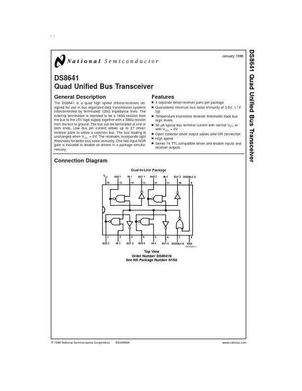
Connection Diagram
Dual-In-Line Package
DS005806-1
Top View Order Number DS8641N See NS Package Number N16A
© 1999 National Semiconductor Corporation
DS005806
.national.
Typical Application
DS005806-2
.national.
Absolute Maximum Ratings (Note 2)
If Military/Aerospace specified devices are required, please contact the National Semiconductor Sales Office/ Distributors for availability and specifications. Supply Voltage 7V Input and Output Voltage 5.5V Storage Temperature Range
- 65˚C to +150˚C Maximum Power Dissipation (Note 1) at 25˚C Cavity Package 1433 m W Molded Package 1362 m W
Lead Temperature (Soldering, 4 seconds)
260˚C
Operating Conditions
Min Supply Voltage, (VCC) DS8641 Temperature Range, (TA) DS8641 4.75 0 Max 5.25 +70 Units V ˚C
Note 1: Derate molded package 10.9 m W/˚C above 25˚C.
Electrical Characteristics
The following apply for VMIN ≤ VCC ≤ VMAX, TMIN ≤ TA ≤ TMAX unless otherwise specified (Note 3) and...