DS90CR218
DS90CR218 is +3.3V Rising Edge Data Strobe LVDS manufactured by National Semiconductor.
Description
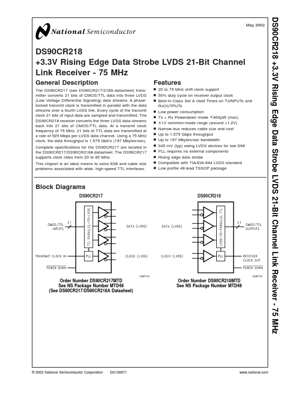
The DS90CR217 (see DS90CR217/218A datasheet) transmitter converts 21 bits of CMOS/TTL data into three LVDS (Low Voltage Differential Signaling) data streams. A phaselocked transmit clock is transmitted in parallel with the data streams over a fourth LVDS link. Every cycle of the transmit clock 21 bits of input data are sampled and transmitted. The DS90CR218 receiver converts the three LVDS data streams back into 21 bits of CMOS/TTL data. At a transmit clock frequency of 75 MHz, 21 bits of TTL data are transmitted at a rate of 525 Mbps per LVDS data channel. Using a 75 MHz clock, the data throughput is 1.575 Gbit/s (197 Mbytes/sec). plete specifications for the DS90CR217 are located in the DS90CR217/DS90CR218A datasheet. The DS90CR217 supports clock rates from 20 to 85 MHz. This chipset is an ideal means to solve EMI and cable size problems associated with wide, high-speed TTL interfaces.
Features n 20 to 75 MHz shift clock support n 50% duty cycle on receiver output clock n Best-in-Class Set & Hold Times on Tx INPUTs and Rx OUTPUTs n Low power consumption n Tx + Rx Powerdown mode < 400µW (max) n ± 1V mon-mode range (around +1.2V) n Narrow bus reduces cable size and cost n Up to 1.575 Gbps throughput n Up to 197 Mbytes/sec bandwidth n 345 m V (typ) swing LVDS devices for low EMI n PLL requires no external ponents n Rising edge data strobe n patible with TIA/EIA-644 LVDS standard n Low profile 48-lead TSSOP package
Block Diagrams
DS90CR217 DS90CR218
Order Number DS90CR217MTD See NS Package Number MTD48 (See DS90CR217/DS90CR218A Datasheet)
Order Number DS90CR218MTD See NS Package Number MTD48
© 2002 National Semiconductor Corporation
DS100871
.national.
Pin Diagram
Typical Application
.national.
Absolute Maximum Ratings
(Note 1)
Package Derating DS90CR218 ESD Rating (HBM, 1.5kΩ, 100p F) (EIAJ, 0Ω, 200p F) Latch Up Tolerance @ 25˚C 15 m W/˚C above +25˚C
If Military/Aerospace...