The following content is an automatically extracted verbatim text
from the original manufacturer datasheet and is provided for reference purposes only.
View original datasheet text
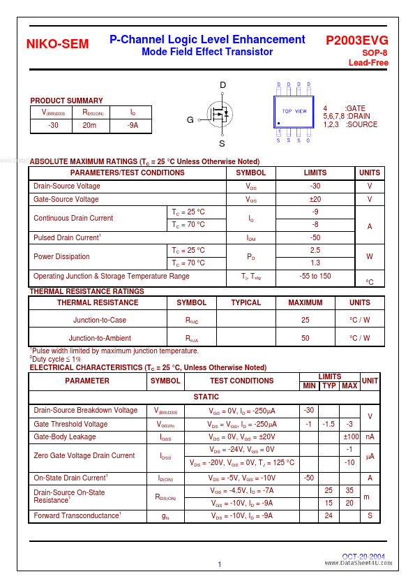
NIKO-SEM
P-Channel Logic Level Enhancement
Mode Field Effect Transistor
D
P2003EVG
SOP-8 Lead-Free
PRODUCT SUMMARY V(BR)DSS -30 RDS(ON) 20m ID -9A
G S
4 :GATE 5,6,7,8 :DRAIN 1,2,3 :SOURCE
www.DataSheet4U.com ABSOLUTE
MAXIMUM RATINGS (TC = 25 °C Unless Otherwise Noted) PARAMETERS/TEST CONDITIONS SYMBOL VDS VGS TC = 25 °C TC = 70 °C ID IDM TC = 25 °C TC = 70 °C PD Tj, Tstg LIMITS -30 ±20 -9 -8 -50 2.5 1.3 -55 to 150 °C UNITS °C / W °C / W W A UNITS V V
Drain-Source Voltage Gate-Source Voltage Continuous Drain Current Pulsed Drain Current Power Dissipation
1
Operating Junction & Storage Temperature Range THERMAL RESISTANCE RATINGS THERMAL RESISTANCE Junction-to-Case Junction-to-Ambient
1 2
SYMBOL RθJc RθJA
TYPICAL
MAXIMUM 25 50
Pulse width limited by maximum junction temperature.