P2003BVT
Overview
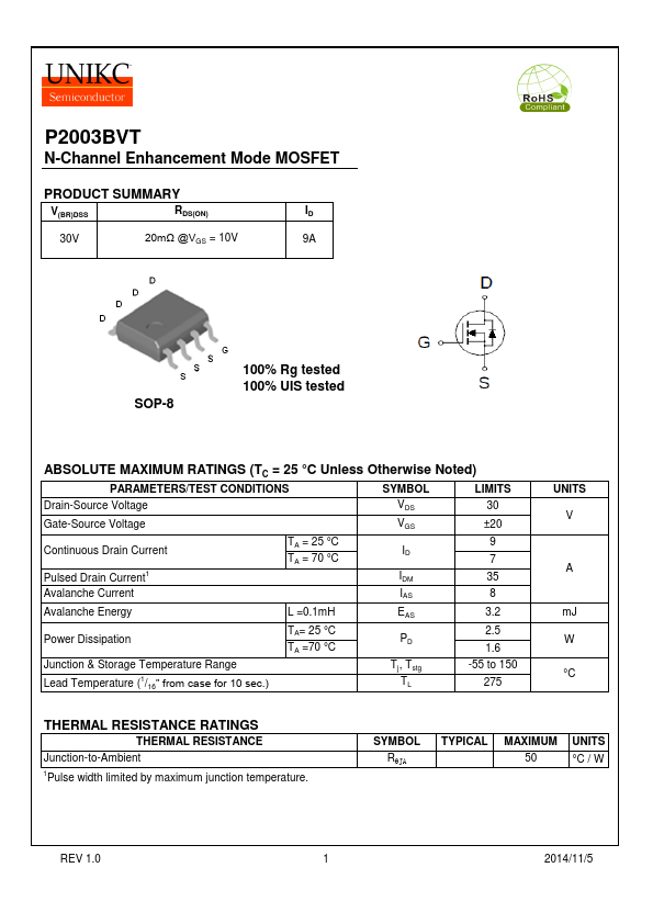
P2003BVT N-Channel Enhancement Mode MOSFET PRODUCT SUMMARY V(BR)DSS RDS(ON) 30V 20mΩ @VGS = 10V ID 9A SOP-8 100% Rg tested 100% UIS tested ABSOLUTE MAXIMUM RATINGS (TC = 25 °C Unless Otherwise...
P2003BVT N-Channel Enhancement Mode MOSFET PRODUCT SUMMARY V(BR)DSS RDS(ON) 30V 20mΩ @VGS = 10V ID 9A SOP-8 100% Rg tested 100% UIS tested ABSOLUTE MAXIMUM RATINGS (TC = 25 °C Unless Otherwise...