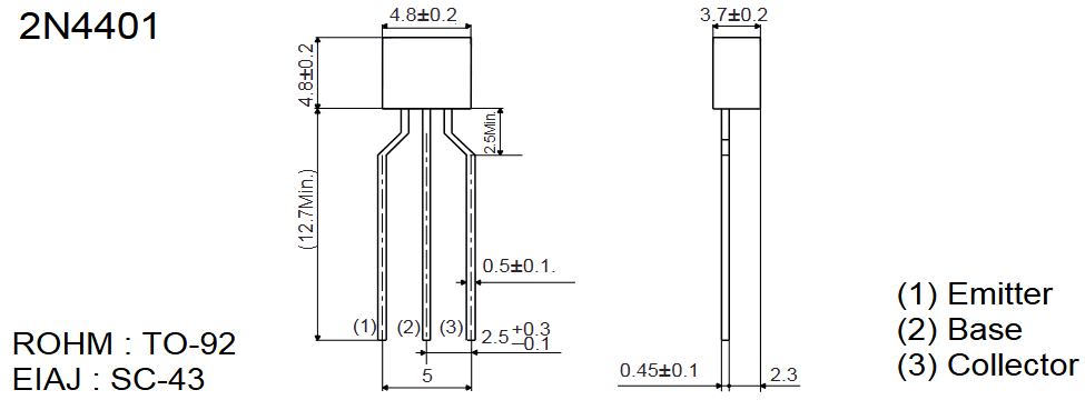
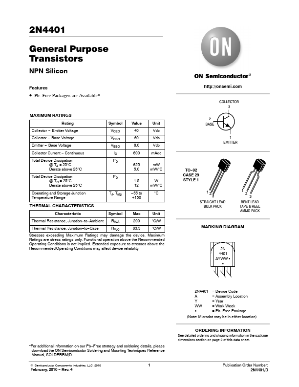
2N4401
Representative 2N4401 image (package may vary by manufacturer)
Overview
- Pb-Free Packages are Available*
| Part | 2N4401 |
|---|---|
| Description | NPN Silicon Transistor |
| Category | Transistor |
| Manufacturer | onsemi |
| Size | 271.66 KB |
Representative 2N4401 image (package may vary by manufacturer)
| Part Number | Manufacturer | Description |
|---|---|---|
| 2N4401 | Inchange Semiconductor | NPN Transistor |
| 2N4401 | General Semiconductor | SMALL SIGNAL TRANSISTORS |
| 2N4401 | ROHM | NPN Medium Power Transistor |
| 2N4401 | Fairchild Semiconductor | NPN General Purpose Amplifier |
| 2N4401 | NXP Semiconductors | NPN switching transistor |