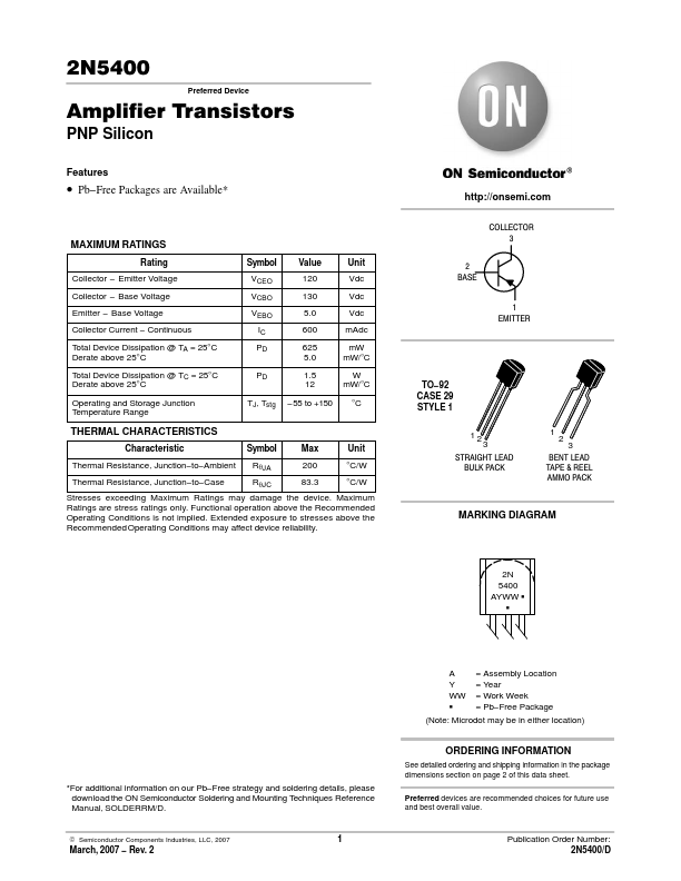
2N5400 Overview
Key Features
- Pb-Free Packages are Available*
| Part | 2N5400 |
|---|---|
| Description | Amplifier Transistor |
| Category | Transistor |
| Manufacturer | onsemi |
| Size | 82.50 KB |
| Part Number | Manufacturer | Description |
|---|---|---|
| 2N5400 | Fairchild Semiconductor | PNP General Purpose Amplifier |
| 2N5400 | Motorola Semiconductor | AMPLIFIER TRANSISTOR |
| 2N5400 | Philips Semiconductors | PNP high-voltage transistors |
| 2N5400 | NTE Electronics | Silicon NPN Transistor |
| 2N5400 | Central Semiconductor | SILICON PNP TRANSISTOR |