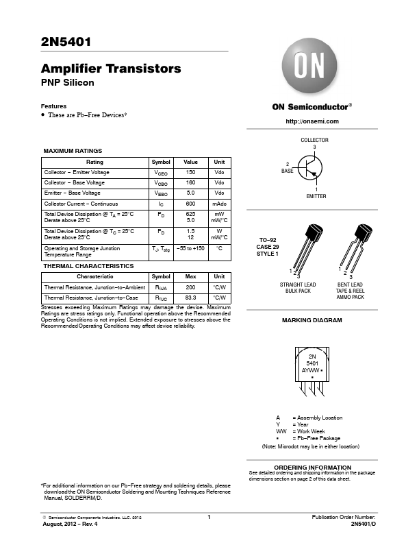
2N5401
Key Features
- These are Pb-Free Devices*
| Part Number | Manufacturer | Description |
|---|---|---|
| 2N5401 | Central Semiconductor | SILICON PNP TRANSISTOR |
| 2N5401 | Inchange Semiconductor | Silicon PNP Power Transistor |
| 2N5401 | Motorola Semiconductor | AMPLIFIER TRANSISTOR |
| 2N5401 | Fairchild Semiconductor | PNP General Purpose Amplifier |
| 2N5401 | Multicomp | Bipolar Transistor |
| 2N5401 | Philips Semiconductors | PNP high-voltage transistors |
| 2N5401C | KEC | PNP TRANSISTOR |
| 2N5401 | Unisonic Technologies | HIGH VOLTAGE SWITCHING TRANSISTOR |
| 2N5401HR | STMicroelectronics | 0.5A PNP transistor |
| 2N5401 | NTE Electronics | Silicon NPN Transistor |