2N5401G Overview
Key Specifications
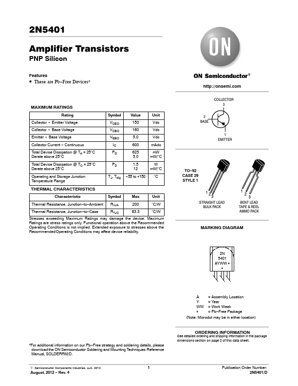
Package: TO-92-3
Pins: 3
Max Frequency: 300 MHz
Height: 5.334 mm
Key Features
- Pb-Free Packages are Available* COLLECTOR 3
| Part | 2N5401G |
|---|---|
| Description | Amplifier Transistors |
| Category | Transistor |
| Manufacturer | onsemi |
| Size | 116.78 KB |
Package: TO-92-3
Pins: 3
Max Frequency: 300 MHz
Height: 5.334 mm
| Seller | Inventory | Price Breaks | Buy |
|---|---|---|---|
| RS (Formerly Allied Electronics) | 0 | 25+ : 0.11 USD | View Offer |
| Component Stockers USA | 679 | 1+ : 99.99 USD | View Offer |
| Part Number | Manufacturer | Description |
|---|---|---|
| 2N5401 | Fairchild Semiconductor | PNP General Purpose Amplifier |
| 2N5401 | Inchange Semiconductor | Silicon PNP Power Transistor |
| 2N5401 | Central Semiconductor | SILICON PNP TRANSISTOR |
| 2N5401 | Motorola Semiconductor | AMPLIFIER TRANSISTOR |
| 2N5401 | Philips Semiconductors | PNP high-voltage transistors |