2N5458G
Features
- N- Channel for Higher Gain
- Drain and Source Interchangeable
- High AC Input Impedance
- High DC Input Resistance
- Low Transfer and Input Capacitance
- Low Cross- Modulation and Intermodulation Distortion
- Plastic Encapsulated Package
- Pb- Free Packages are Available-
MAXIMUM RATINGS
Rating
Symbol
Value
Unit
Drain
- Source Voltage Drain
- Gate Voltage Reverse Gate
- Source Voltage Gate Current Total Device Dissipation @ TA = 25°C Derate above 25°C
VDS VDG VGSR IG PD
Vdc
Vdc
- 25
Vdc
10 m Adc
310 m W
2.82 m W/°C
Operating Junction Temperature
°C
Storage Temperature Range
Tstg
- 65 to +150 °C
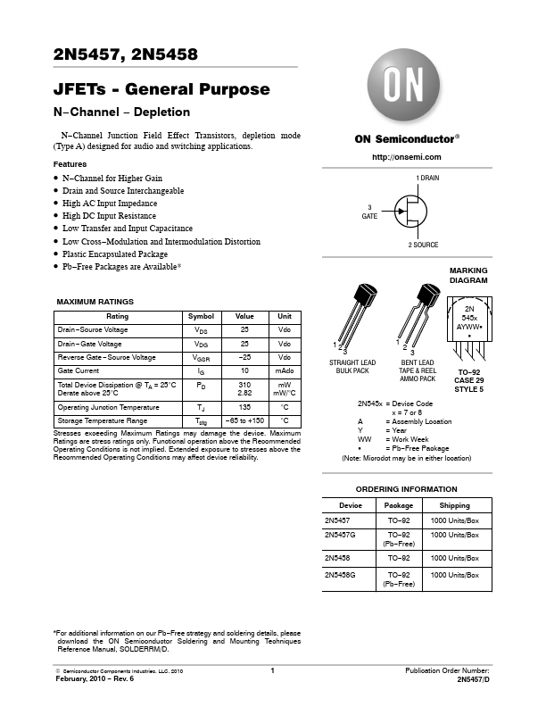
Stresses exceeding Maximum Ratings may damage the device. Maximum Ratings are stress ratings only. Functional operation above the Remended Operating Conditions is not implied. Extended exposure to stresses above the Remended Operating Conditions may affect device reliability. http://onsemi. 1 DRAIN
3 GATE
2 SOURCE
MARKING DIAGRAM
STRAIGHT LEAD...