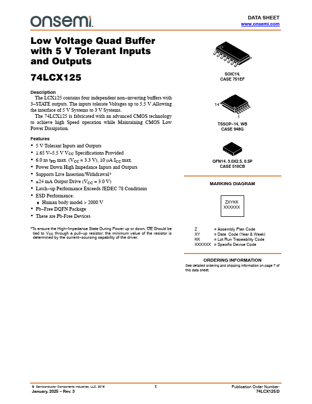
74LCX125 Datasheet Text
Low Voltage Quad Buffer with 5 V Tolerant Inputs and Outputs
74LCX125
Description The LCX125 contains four independent non- inverting buffers with
3- STATE outputs. The inputs tolerate Voltages up to 5.5 V Allowing the interface of 5 V Systems to 3 V Systems.
The 74LCX125 is fabricated with an advanced CMOS technology to achieve high Speed operation while Maintaining CMOS Low Power Dissipation.
Features
- 5 V Tolerant Inputs and Outputs
- 1.65 V- 5.5 V VCC Specifications Provided
- 6.0 ns tPD max. (VCC = 3.3 V), 10 mA ICC max.
- Power Down High Impedance Inputs and Outputs
- Supports Live Insertion/Withdrawal-
- 24 mA Output Drive (VCC = 3.0 V)
- Latch- up Performance Exceeds JEDEC 78 Conditions
- ESD Performance:
Human body model > 2000 V
- Pb- Free DQFN Package
- These are Pb-Free Devices
- To ensure the High- Impedance State During Power up or down, OE Should be tied to VCC through a pull- up resistor: the minimum value of the resistor is determined by the current- sourcing capability of the driver.
DATA SHEET .onsemi.
SOIC14, CASE 751EF
14 1
TSSOP- 14, WB CASE 948G
QFN14, 3.0X2.5, 0.5P CASE 510CB
MARKING DIAGRAM
ZXYKK XXXXXX
Z
= Assembly Plan Code
XY
= Date Code (Year & Week)
KK...