74VCX16244 Overview
Key Specifications
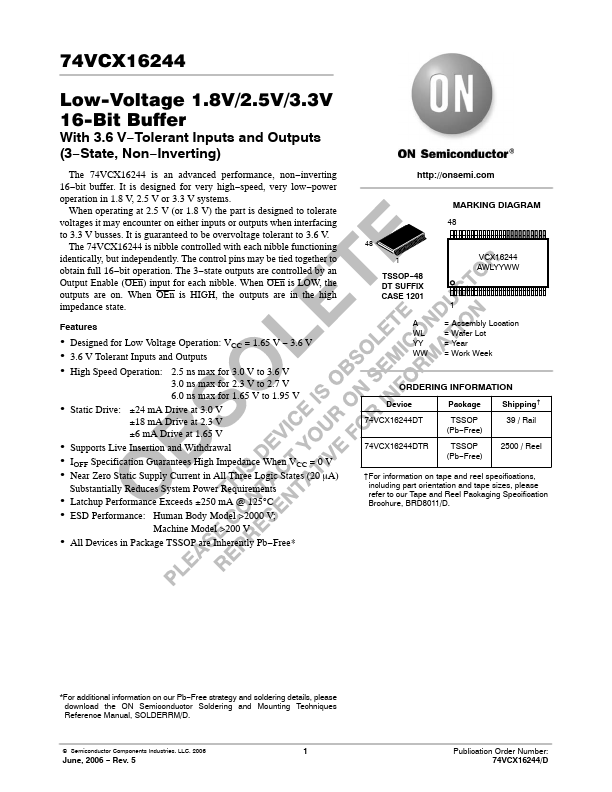
Package: TSSOP
Mount Type: Surface Mount
Pins: 48
Operating Voltage: 1.5 V
Key Features
- Designed for Low Voltage Operation: VCC = 1.65 V
- 3.6 V Tolerant Inputs and Outputs
- High Speed Operation: 2.5 ns max for 3.0 V to 3.6 V