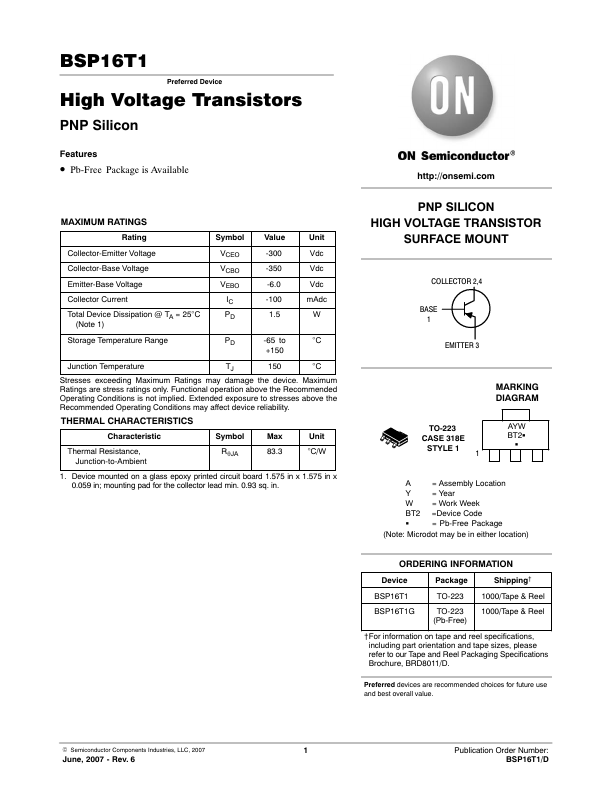
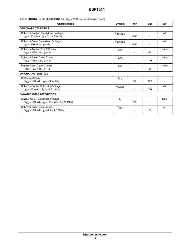
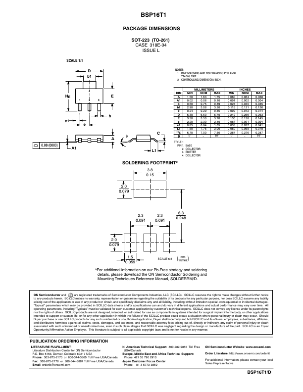
The following content is an automatically extracted verbatim text
from the original manufacturer datasheet and is provided for reference purposes only.
View original datasheet text
BSP16T1
Preferred Device
High Voltage Transistors
PNP Silicon
Features
•ăPb-Free Package is Available
MAXIMUM RATINGS
Rating
Symbol Value
Unit
Collector‐Emitter Voltage
Collector‐Base Voltage
Emitter‐Base Voltage
Collector Current Total Device Dissipation @ TA = 25°C
(Note 1)
VCEO VCBO VEBO
IC PD
-300 -350 -6.0 -100 1.5
Vdc Vdc Vdc mAdc W
Storage Temperature Range
PD
-65 to
°C
+150
Junction Temperature
TJ 150 °C
Stresses exceeding Maximum Ratings may damage the device. Maximum Ratings are stress ratings only. Functional operation above the Recommended Operating Conditions is not implied. Extended exposure to stresses above the Recommended Operating Conditions may affect device reliability.