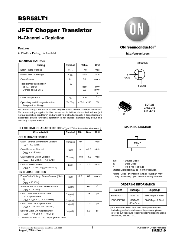
BSR58LT1 Overview
Key Features
- Pb-Free Package is Available
| Part | BSR58LT1 |
|---|---|
| Description | N-Channel Transistor |
| Category | Transistor |
| Manufacturer | onsemi |
| Size | 88.19 KB |
| Part Number | Manufacturer | Description |
|---|---|---|
| BSR58 | Fairchild Semiconductor | N-Channel Low-Frequency Low Noise Amplifier |
| BSR58 | NXP Semiconductors | N-channel FETs |