BUL45D2
BUL45D2 is NPN Transistor manufactured by onsemi.
BUL45 NPN Silicon Power Transistor
High Voltage SWITCHMODEt Series
Designed for use in electronic ballast (light ballast) and in Switchmode Power supplies up to 50 Watts.
Features http://onsemi.
- Improved Efficiency Due to:
Low Base Drive Requirements (High and Flat DC Current Gain h FE) Low Power Losses (On- State and Switching Operations)
- Fast Switching: tfi = 100 ns (typ) and tsi = 3.2 ms (typ)
- @ IC = 2.0 A, IB1 = IB2 = 0.4 A Full Characterization at 125°C Tight Parametric Distributions Consistent Lot- to- Lot Pb- Free Package is Available-
- -
POWER TRANSISTOR 5.0 AMPERES, 700 VOLTS, 35 AND 75 WATTS
- -
- MAXIMUM RATINGS
Rating Collector- Emitter Sustaining Voltage Collector- Base Breakdown Voltage
..
Symbol VCEO VCES VEBO IC ICM IB PD TJ, Tstg
Value 400 700 9.0 5.0 10 2.0 75 0.6
- 65 to 150
Unit Vdc Vdc Vdc Adc Adc W W/_C _C
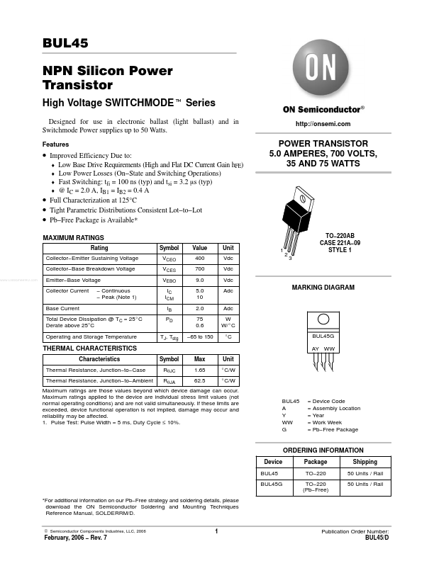
TO- 220AB CASE 221A- 09 STYLE 1 3
Emitter- Base Voltage Collector Current Base Current Total Device Dissipation @ TC = 25_C Derate above 25°C Operating and Storage Temperature
- Continuous
- Peak (Note 1)
MARKING DIAGRAM
BUL45G AY WW
THERMAL CHARACTERISTICS
Characteristics Thermal Resistance, Junction- to- Case Thermal Resistance, Junction- to- Ambient Symbol Rq JC Rq JA Max 1.65 62.5 Unit _C/W _C/W
Maximum ratings are those values beyond which device damage can occur. Maximum ratings applied to the device are individual stress limit values (not normal operating conditions) and are not valid simultaneously. If these limits are exceeded, device functional operation is not implied, damage may occur and reliability may be affected. 1. Pulse Test: Pulse Width = 5 ms, Duty Cycle ≤ 10%.
BUL45 A Y WW G
= Device Code = Assembly Location = Year = Work Week = Pb- Free Package
ORDERING...