Datasheet4U Logo Datasheet4U.com

CAT24C05 - 2-Kb and 4-Kb I2C Serial EEPROM

Download the CAT24C05 datasheet PDF. This datasheet also covers the CAT24C03 variant, as both devices belong to the same 2-kb and 4-kb i2c serial eeprom family and are provided as variant models within a single manufacturer datasheet.

General Description

The CAT24C03/05 is a 2 Kb/4

organized internally as 16/32 pages of 16 bytes each, for a total of 256x8/512x8 bits.

These devices support both Standard (100 kHz) as well as Fast (400 kHz) I2C protocol.

Key Features

  • Supports Standard and Fast I2C Protocol.
  • 1.8 V to 5.5 V Supply Voltage Range.
  • 16.
  • Byte Page Write Buffer.
  • Hardware Write Protection for Upper Half of Memory.
  • Schmitt Triggers and Noise Suppression Filters on I2C Bus Inputs (SCL and SDA).
  • Low Power CMOS Technology.
  • 1,000,000 Program/Erase Cycles.
  • 100 Year Data Retention.
  • Industrial Temperature Range.
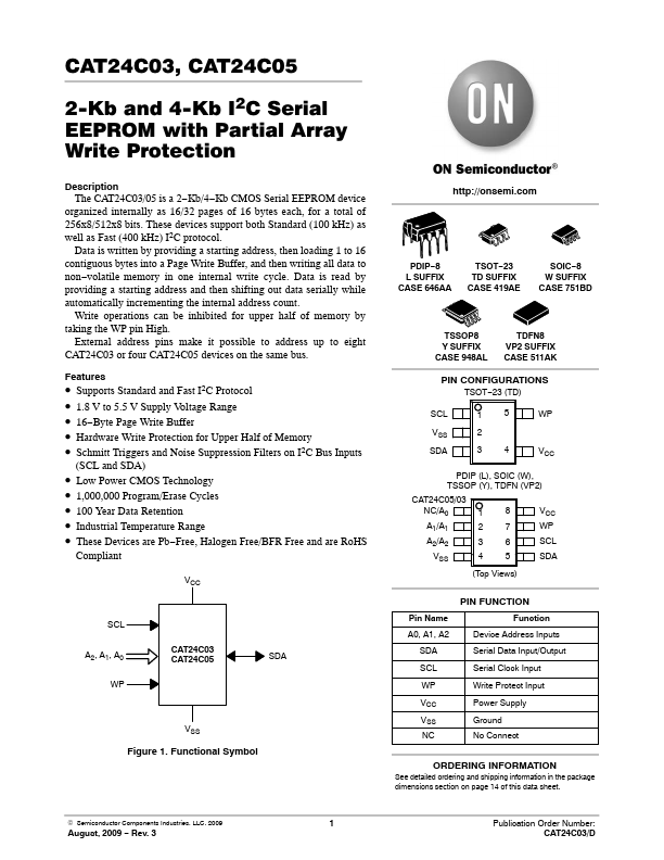
  • These Devices are Pb.
  • Free, Halogen Free/BF.

📥 Download Datasheet

Note: The manufacturer provides a single datasheet file (CAT24C03-ONSemiconductor.pdf) that lists specifications for multiple related part numbers.

Datasheet Details

Part number CAT24C05
Manufacturer onsemi
File Size 159.62 KB
Description 2-Kb and 4-Kb I2C Serial EEPROM
Datasheet download datasheet CAT24C05 Datasheet

Full PDF Text Transcription (Reference)

The following content is an automatically extracted verbatim text from the original manufacturer datasheet and is provided for reference purposes only.

View original datasheet text
CAT24C03, CAT24C05 2-Kb and 4-Kb I2C Serial EEPROM with Partial Array Write Protection Description The CAT24C03/05 is a 2−Kb/4−Kb CMOS Serial EEPROM device organized internally as 16/32 pages of 16 bytes each, for a total of 256x8/512x8 bits. These devices support both Standard (100 kHz) as well as Fast (400 kHz) I2C protocol. Data is written by providing a starting address, then loading 1 to 16 contiguous bytes into a Page Write Buffer, and then writing all data to non−volatile memory in one internal write cycle. Data is read by providing a starting address and then shifting out data serially while automatically incrementing the internal address count. Write operations can be inhibited for upper half of memory by taking the WP pin High.