FDG1024NZ
FDG1024NZ is Dual N-Channel MOSFET manufactured by onsemi.
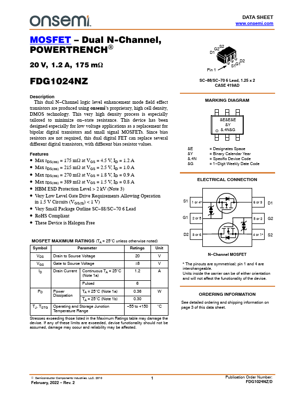
MOSFET
- Dual N-Channel, POWERTRENCH®
20 V, 1.2 A, 175 mW
Description This dual N- Channel logic level enhancement mode field effect transistors are produced using onsemi’s proprietary, high cell density, DMOS technology. This very high density process is especially tailored to minimize on- state resistance. This device has been designed especially for low voltage applications as a replacement for bipolar digital transistors and small signal MOSFETs. Since bias resistors are not required, this dual digital FET can replace several different digital transistors, with different bias resistor values.
Features
- Max rDS(on) = 175 mW at VGS = 4.5 V, ID = 1.2 A
- Max rDS(on) = 215 mW at...