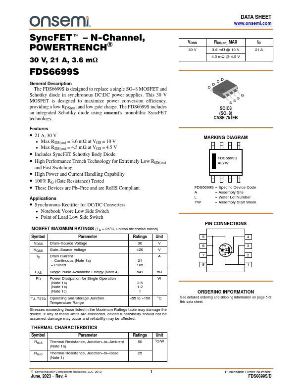
FDS6699S
FDS6699S is N-Channel MOSFET manufactured by onsemi.
Description
The FDS6699S is designed to replace a single SO- 8 MOSFET and
Schottky diode in synchronous DC:DC power supplies. This 30 V MOSFET is designed to maximize power conversion efficiency, providing a low RDS(on) and low gate charge. The FDS6699S includes an integrated Schottky diode using onsemi’s monolithic Sync FET technology.
Features
- 21 A, 30 V
- Max RDS(on) = 3.6 m W at VGS = 10 V
- Max RDS(on) = 4.5 m W at VGS = 4.5 V
- Includes Sync FET Schottky Body Diode
- High Performance Trench Technology for Extremely Low RDS(on) and Fast Switching
- High Power and Current Handling Capability
- 100% RG (Gate Resistance) Tested
- These Devices are Pb- Free and are Ro HS pliant
Applications
- Synchronous Rectifier for DC/DC Converters
- Notebook Vcore Low Side Switch
- Point of Load Low Side Switch
MOSFET MAXIMUM RATINGS (TA = 25°C, unless otherwise noted)
Symbol VDSS VGSS ID
Parameter
Drain- Source Voltage
Gate- Source Voltage
Drain Current
- Continuous (Note 1a)
- Pulsed
Ratings Unit
±20
A 21 105
EAS Single Pulse Avalanche Energy (Note 4)
PD Power Dissipation for Single Operation (Note 1a) (Note 1b) (Note 1c)
TJ, TSTG Operating and Storage Junction Temperature Range
541 m J
W 2.5 1.2 1
- 55 to +150 °C
Stresses exceeding those listed in the Maximum Ratings table may damage the device. If any of these limits are exceeded, device functionality should not be assumed, damage may occur and reliability may be affected.
THERMAL CHARACTERISTICS
Symbol
Parameter
Rq JA Thermal Resistance, Junction- to- Ambient (Note...