FDT86102LZ
Description
This N- Channel MOSFET is produced using onsemi’s advanced
POWERTRENCH process that has been especially tailored to minimize the on- state resistance and switching loss. G- S zener has been added to enhance ESD voltage level.
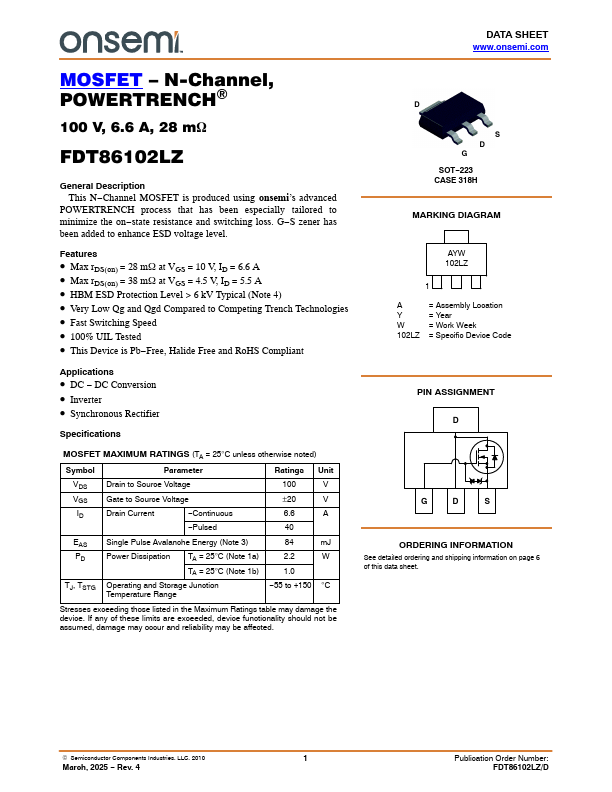
S D G SOT- 223 CASE 318H
MARKING DIAGRAM
Features
- Max r DS(on) = 28 m W at VGS = 10 V, ID = 6.6 A
- Max r DS(on) = 38 m W at VGS = 4.5 V, ID = 5.5 A
- HBM ESD Protection Level > 6 k V Typical (Note 4)
- Very Low Qg and Qgd pared to peting Trench Technologies
- Fast Switching Speed
- 100% UIL Tested
- This Device is Pb- Free, Halide Free and Ro HS pliant
AYW 102LZ
A Y W 102LZ
= Assembly Location = Year = Work Week = Specific Device Code
Applications
- DC
- DC Conversion
- Inverter
- Synchronous Rectifier
Specifications
PIN ASSIGNMENT D
MOSFET MAXIMUM RATINGS (TA = 25°C unless otherwise noted)
Symbol
Parameter
Ratings Unit
VDS Drain to Source Voltage
VGS Gate to Source Voltage
Drain Current
- Continuous
-...