FIN1019 Overview
Key Specifications
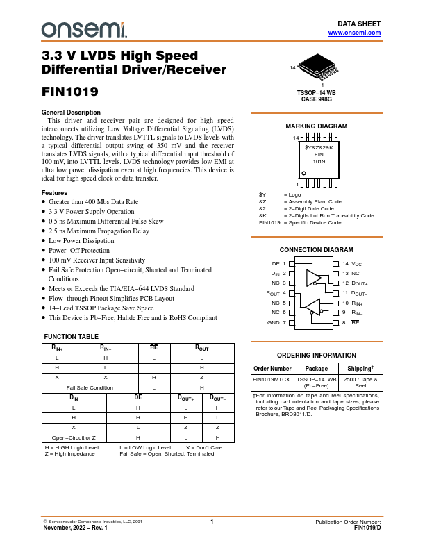
Package: TSSOP
Mount Type: Surface Mount
Pins: 14
Operating Voltage: 3.3 V
Description
This driver and receiver pair are designed for high speed interconnects utilizing Low Voltage Differential Signaling (LVDS) technology. The driver translates LVTTL signals to LVDS levels with a typical differential output swing of 350 mV and the receiver translates LVDS signals, with a typical differential input threshold of 100 mV, into LVTTL levels.
Key Features
- Greater than 400 Mbs Data Rate
- 3.3 V Power Supply Operation
- 0.5 ns Maximum Differential Pulse Skew
- 2.5 ns Maximum Propagation Delay
- Low Power Dissipation
- Power-Off Protection
- 100 mV Receiver Input Sensitivity
- Fail Safe Protection Open-circuit, Shorted and Terminated Conditions
- Meets or Exceeds the TIA/EIA-644 LVDS Standard
- Flow-through Pinout Simplifies PCB Layout