FNB80560T3
FNB80560T3 is Motion SPM8 Module manufactured by onsemi.
Motion SPM) 8 Series
FNB80560T3 is a Motion SPM 8 module providing a fully- featured, high- performance inverter output stage for AC Induction, BLDC, and PMSM motors. These modules integrate optimized gate drive of the built- in IGBTs to minimize EMI and losses, while also providing multiple on- module protection Features including under- voltage lockouts, inter- lock function, over- current shutdown, thermal monitoring of drive IC, and fault reporting. The built- in, high- speed HVIC requires only a single supply voltage and translates the ining logic- level gate inputs to the high- voltage, high- current drive signals required to properly drive the module’s robust shortcircuit- rated IGBTs. Separate negative IGBT terminals are available for each phase to support the widest variety of control algorithms.
.onsemi.
Features
- UL Certified No. E209204 (UL1557)
- 600 V
- 5 A 3- Phase IGBT Inverter Including Control IC for Gate
Drive and Protections
- Low- Loss, Short- Circuit Rated IGBTs
- Separate Open- Emitter Pins from Low- Side IGBTs for Three- Phase
Current Sensing
- Active- high Interface, works with 3.3 / 5 V Logic, Schmitt- trigger
Input
- HVIC for Gate Driving, Under- Voltage and Short- Circuit Current
Protection
- Fault Output for Under- Voltage and Short- Circuit Current Protection
- Inter- Lock Function to Prevent Short- Circuit
- Shut- Down Input
- HVIC Temperature- Sensing Built- In for Temperature Monitoring
- Isolation Rating: 1500 Vrms / min.
Applications
- Motion Control
- Home Appliance / Industrial Motor
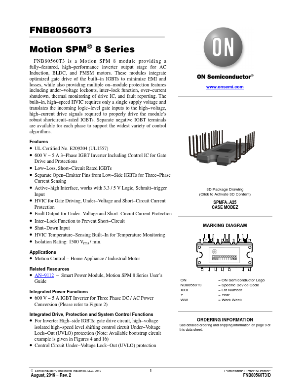
3D Package Drawing (Click to Activate 3D Content)
SPMFA- A25 CASE MODEZ
MARKING DIAGRAM
Related Resources
- AN- 9112
- Smart Power Module, Motion SPM 8 Series...