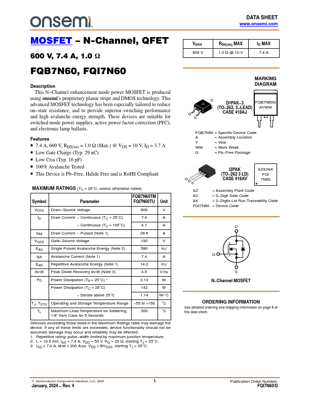
FQB7N60
FQB7N60 is N-Channel MOSFET manufactured by onsemi.
Description
This N- Channel enhancement mode power MOSFET is produced using onsemi’s proprietary planar stripe and DMOS technology. This advanced MOSFET technology has been especially tailored to reduce on- state resistance, and to provide superior switching performance and high avalanche energy strength. These devices are suitable for switched mode power supplies, active power factor correction (PFC), and electronic lamp ballasts.
Features
- 7.4 A, 600 V, RDS(on) = 1.0 W (Max.) @ VGS = 10 V, ID = 3.7 A
- Low Gate Charge (Typ. 29 n C)
- Low Crss (Typ. 16 p F)
- 100% Avalanche Tested
- This Device is Pb- Free, Halide Free and is Ro HS pliant
MAXIMUM RATINGS (TC = 25°C, unless otherwise noted)
Symbol
Parameter
FQB7N60TM FQI7N60TU Unit
VDSS ID
IDM VGSS EAS
IAR EAR dv/dt
Drain- Source Voltage Drain Current
- Continuous (TC = 25°C)
- Continuous (TC = 100°C) Drain Current
- Pulsed (Note 1) Gate- Source Voltage Single Pulsed Avalanche Energy (Note 2) Avalanche Current (Note 1) Repetitive Avalanche Energy (Note 1) Peak Diode Recovery dv/dt (Note 3)
±30
580 m J
14.2 m J
V/ns
PD Power Dissipation (TA = 25°C)
- Power Dissipation (TC = 25°C)
- Derate above 25°C
W/°C
TJ, TSTG Operating and Storage Temperature Range
- 55 to +150 °C
TL Maximum Lead Temperature for Soldering,
°C
1/8” from Case for 5 Seconds
Stresses exceeding those listed in the Maximum Ratings table may damage the device. If any of these limits are exceeded, device functionality should not be assumed, damage may occur and reliability may be affected.
1. Repetitive rating: pulse- width limited by maximum junction temperature. 2. L = 19.5 m H, IAS = 7.4 A, VDD = 50 V, RG = 25 W, starting TJ = 25°C. 3. ISD ≤ 7.4 A, di/dt ≤ 200 A/ms, VDD ≤ BVDSS, starting TJ =...