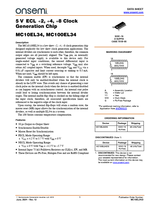
Datasheet4U Logo Datasheet4U.com

MC100EL34 - Clock Generation Chip

General Description

designed explicitly for low skew clock generation applications.

The internal dividers are synchronous to each other, therefore, the common output edges are all precisely aligned.

Key Features

  • 50 ps Output-to-Output Skew.
  • Synchronous Enable/Disable.
  • Master Reset for Synchronization.
  • PECL Mode Operating Range:.
  • VCC = 4.2 V to 5.7 V with VEE = 0 V.
  • NECL Mode Operating Range:.
  • VCC = 0 V with VEE =.
  • 4.2 V to.
  • 5.7 V.
  • Internal Input 75 kW Pulldown Resistors on CLK(s), EN, and MR.
  • These Devices are Pb-Free, Halogen Free and are RoHS Compliant DATA SHEET www. onsemi. com 16 1 SOIC.
  • 16 D SU.

📥 Download Datasheet

Datasheet Details

Part number MC100EL34
Manufacturer onsemi
File Size 265.53 KB
Description Clock Generation Chip
Datasheet download datasheet MC100EL34 Datasheet

Full PDF Text Transcription (Reference)

The following content is an automatically extracted verbatim text from the original manufacturer datasheet and is provided for reference purposes only.

View original datasheet text
5 V ECL P2, P4, P8 Clock Generation Chip MC10EL34, MC100EL34 Description The MC10/100EL34 is a low skew ÷2, ÷4, ÷8 clock generation chip designed explicitly for low skew clock generation applications. The internal dividers are synchronous to each other, therefore, the common output edges are all precisely aligned. The VBB pin, an internally generated voltage supply, is available to this device only. For single-ended input conditions, the unused differential input is connected to VBB as a switching reference voltage. VBB may also rebias AC coupled inputs. When used, decouple VBB and VCC via a 0.01 mF capacitor and limit current sourcing or sinking to 0.5 mA. When not used, VBB should be left open.