Datasheet4U Logo Datasheet4U.com

MC100EP91 - NECL Output Translator

Description

translator.

3.0 V/

5.5 V).

Features

  • Maximum Input Clock Frequency = > 2.0 GHz Typical.
  • Maximum Input Data Rate = > 2.0 Gb/s Typical.
  • 500 ps Typical Propagation Delay.
  • Operating Range: VCC = 2.375 V to 3.8 V; VEE =.
  • 3.0 V to.
  • 5.5 V; GND = 0 V.
  • Q Output will Default LOW with Inputs Open or at GND.
  • These Devices are Pb-Free, Halogen Free and are RoHS Compliant www. onsemi. com 20 1 SOIC.
  • 20 WB DW SUFFIX CASE 751D 24 1 QFN.
  • 24 MN SUFFIX CASE 485L MA.

📥 Download Datasheet

Datasheet Details

Part number MC100EP91
Manufacturer onsemi
File Size 354.69 KB
Description NECL Output Translator
Datasheet download datasheet MC100EP91 Datasheet

Full PDF Text Transcription (Reference)

The following content is an automatically extracted verbatim text from the original manufacturer datasheet and is provided for reference purposes only.

View original datasheet text
2.5 V/3.3 V Any Level Positive Input to -3.3 V/-5.5 V NECL Output Translator 
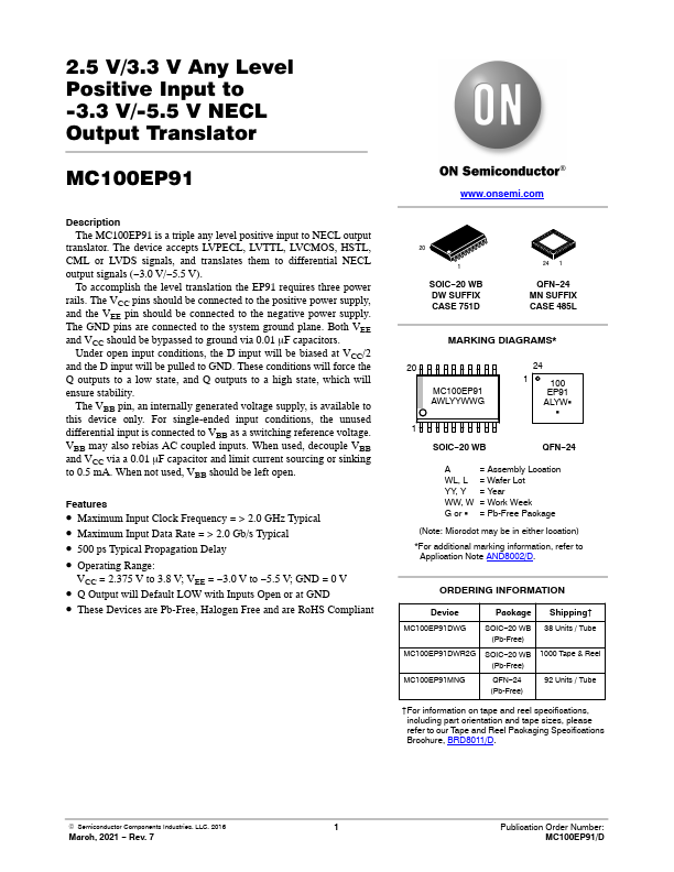
MC100EP91 Description 
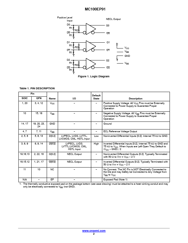
The MC100EP91 is a triple any level positive input to NECL output translator. The device accepts LVPECL, LVTTL, LVCMOS, HSTL, CML or LVDS signals, and translates them to differential NECL output signals (−3.0 V/−5.5 V). To accomplish the level translation the EP91 requires three power rails. The VCC pins should be connected to the positive power supply, and the VEE pin should be connected to the negative power supply. The GND pins are connected to the system ground plane. Both VEE and VCC should be bypassed to ground via 0.01 mF capacitors. Under open input conditions, the D input will be biased at VCC/2 and the D input will be pulled to GND.
Published: |