MC10EL15 Overview
Key Specifications
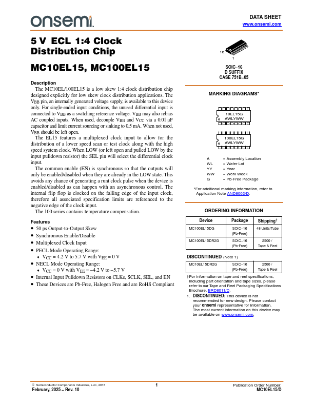
Package: SOP
Operating Voltage: 5 V
Max Voltage (typical range): 5.7 V
Min Voltage (typical range): 4.2 V
Description
The MC10EL/100EL15 is a low skew 1:4 clock distribution chip designed explicitly for low skew clock distribution applications. The VBB pin, an internally generated voltage supply, is available to this device only.
Key Features
- 50 ps Output-to-Output Skew
- Synchronous Enable/Disable
- Multiplexed Clock Input
- PECL Mode Operating Range
- VCC = 4.2 V to 5.7 V with VEE = 0 V
- NECL Mode Operating Range
- VCC = 0 V with VEE = -4.2 V to -5.7 V
- Internal Input Pulldown Resistors on CLKs, SCLK, SEL, and EN