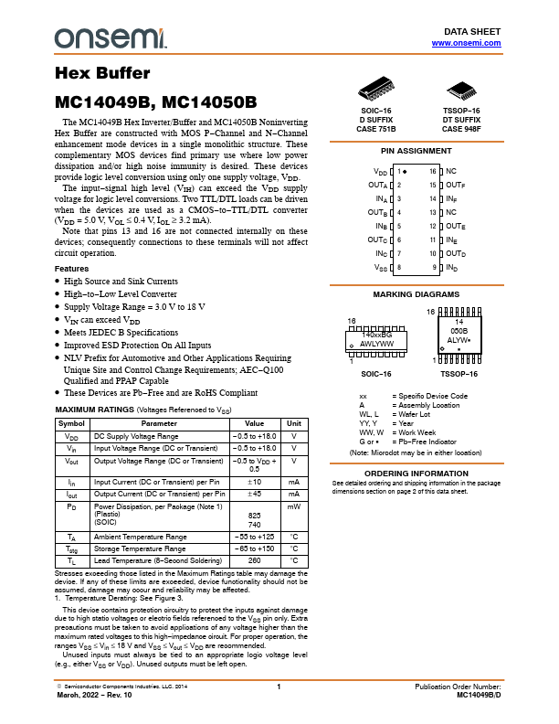
Datasheet4U Logo Datasheet4U.com

MC14049B - Hex Buffer

Key Features

  • High Source and Sink Currents.
  • High.
  • to.
  • Low Level Converter.
  • Supply Voltage Range = 3.0 V to 18 V.
  • VIN can exceed VDD.
  • Meets JEDEC B Specifications.
  • Improved ESD Protection On All Inputs.
  • NLV Prefix for Automotive and Other.

📥 Download Datasheet

Full PDF Text Transcription (Reference)

The following content is an automatically extracted verbatim text from the original manufacturer datasheet and is provided for reference purposes only.

View original datasheet text
Hex Buffer MC14049B, MC14050B The MC14049B Hex Inverter/Buffer and MC14050B Noninverting Hex Buffer are constructed with MOS P−Channel and N−Channel enhancement mode devices in a single monolithic structure. These complementary MOS devices find primary use where low power dissipation and/or high noise immunity is desired. These devices provide logic level conversion using only one supply voltage, VDD. The input−signal high level (VIH) can exceed the VDD supply voltage for logic level conversions. Two TTL/DTL loads can be driven when the devices are used as a CMOS−to−TTL/DTL converter (VDD = 5.0 V, VOL ≤ 0.4 V, IOL ≥ 3.2 mA). Note that pins 13 and 16 are not connected internally on these devices; consequently connections to these terminals will not affect circuit operation.