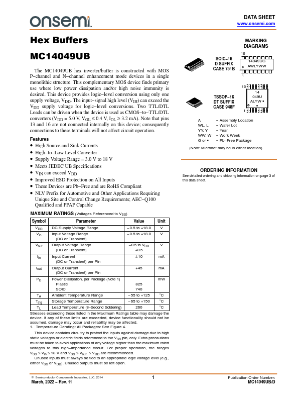
- Part: MC14049UB
- Description: Hex Buffers
- Manufacturer: onsemi
- Size: 195.55 KB
Key Features
- High Source and Sink Currents
- High-to-Low Level Converter
- Supply Voltage Range = 3.0 V to 18 V
- Meets JEDEC UB Specifications
- VIN can exceed VDD
- Improved ESD Protection on All Inputs
- These Devices are Pb-Free and are RoHS compliant
- NLV Prefix for Automotive and Other Applications Requiring Unique Site and Control Change Requirements; AEC-Q100 Qualified and PPAP Capable
Datasheets by Manufacturer
| Part Number |
Manufacturer |
Description |
|
MC14049B
|
Motorola Semiconductor |
Hex Buffer |
|
MC14043B
|
Motorola Semiconductor |
CMOS MSI |
|
MC14042B
|
Motorola Semiconductor |
Quad Transparent Latch |
|
MC1404A
|
Motorola Semiconductor |
Voltage Reference |
|
MC14040B
|
Motorola Semiconductor |
12-Bit Binary Counter |
|
MC14046B
|
Motorola Semiconductor |
Phase Locked Loop |
|
MC1404
|
Motorola Semiconductor |
Voltage Reference |


