MC74AC174
MC74AC174 is manufactured by onsemi.
MC74AC174, MC74ACT174 Hex D Flip- Flop with Master Reset
The MC74AC174/74ACT174 is a high- speed hex D flip- flop. The device is used primarily as a 6- bit edge- triggered storage register. The information on the D inputs is transferred to storage during the LOW- to- HIGH clock transition. The device has a Master Reset to simultaneously clear all flip- flops. http://onsemi.
- Outputs Source/Sink 24 mA
- ′ACT174 Has TTL patible Inputs
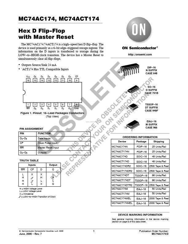
VCC 16 Q5 15 D5 14 D4 13 Q4 12 D3 11 Q3 10 CP 9
16 1
DIP- 16 N SUFFIX CASE 648
SO- 16 D SUFFIX CASE 751B
1 MR
2 Q0
3 D0
4 D1
5 Q1
6 D2
7 Q2
8 GND
Figure 1. Pinout: 16- Lead Packages Conductors (Top View)
..
TSSOP- 16 DT...