Datasheet4U Logo Datasheet4U.com

MC74AC273 - Octal D Flip-Flop

Download the MC74AC273 datasheet PDF. This datasheet also covers the MC74ACT273 variant, as both devices belong to the same octal d flip-flop family and are provided as variant models within a single manufacturer datasheet.

Key Features

  • Ideal Buffer for MOS Microprocessor or Memory.
  • Eight Edge-Triggered D Flip.
  • Flops.
  • Buffered Common Clock.
  • Buffered, Asynchronous Master Reset.
  • See MC74AC377 for Clock Enable Version.
  • See MC74AC373 for Transparent Latch Version.
  • See MC74AC374 for 3-State Version.
  • Outputs Source/Sink 24 mA.
  • ′ACT273 Has TTL Compatible Inputs.
  • These are Pb.
  • Free Devices 
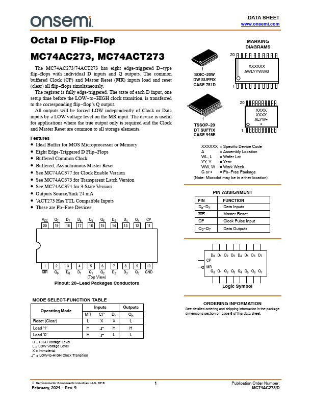
VCC Q7 D7 D6 Q6 Q5 D5 D4 Q4 CP 20 19 18 17.

📥 Download Datasheet

Note: The manufacturer provides a single datasheet file (MC74ACT273_ONSemiconductor.pdf) that lists specifications for multiple related part numbers.

Datasheet Details

Part number MC74AC273
Manufacturer onsemi
File Size 263.35 KB
Description Octal D Flip-Flop
Datasheet download datasheet MC74AC273 Datasheet

Full PDF Text Transcription (Reference)

The following content is an automatically extracted verbatim text from the original manufacturer datasheet and is provided for reference purposes only.

View original datasheet text
Octal D Flip-Flop MC74AC273, MC74ACT273 The MC74AC273/74ACT273 has eight edge-triggered D−type flip−flops with individual D inputs and Q outputs. The common buffered Clock (CP) and Master Reset (MR) inputs load and reset (clear) all flip−flops simultaneously. The register is fully edge-triggered. The state of each D input, one setup time before the LOW−to−HIGH clock transition, is transferred to the corresponding flip−flop’s Q output. All outputs will be forced LOW independently of Clock or Data inputs by a LOW voltage level on the MR input. The device is useful for applications where the true output only is required and the Clock and Master Reset are common to all storage elements.