Datasheet4U Logo Datasheet4U.com

MC74ACT174 - Hex D Flip-Flop

Download the MC74ACT174 datasheet PDF. This datasheet also covers the MC74AC174 variant, as both devices belong to the same hex d flip-flop family and are provided as variant models within a single manufacturer datasheet.

General Description

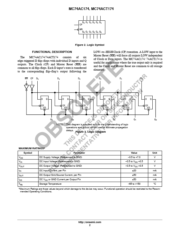
The MC74AC174/74ACT174 consists of six edge triggered D flip

flops with individual D inputs and Q outputs.

flops.

flop’s output following the MR C

Key Features

  • Recovery Time MR to CP.
  • Voltage Range 5.0 V is 5.0 V ±0.5 V.

📥 Download Datasheet

Note: The manufacturer provides a single datasheet file (MC74AC174_ONSemiconductor.pdf) that lists specifications for multiple related part numbers.

Full PDF Text Transcription (Reference)

The following content is an automatically extracted verbatim text from the original manufacturer datasheet and is provided for reference purposes only.

View original datasheet text
MC74AC174, MC74ACT174 Hex D Flip−Flop with Master Reset The MC74AC174/74ACT174 is a high−speed hex D flip−flop. The device is used primarily as a 6−bit edge−triggered storage register. The information on the D inputs is transferred to storage during the LOW−to−HIGH clock transition. The device has a Master Reset to simultaneously clear all flip−flops. http://onsemi.com • Outputs Source/Sink 24 mA • ′ACT174 Has TTL Compatible Inputs VCC 16 Q5 15 D5 14 D4 13 Q4 12 D3 11 Q3 10 CP 9 16 1 DIP−16 N SUFFIX CASE 648 16 1 SO−16 D SUFFIX CASE 751B 1 MR 2 Q0 3 D0 4 D1 5 Q1 6 D2 7 Q2 8 GND 16 Figure 1. Pinout: 16−Lead Packages Conductors (Top View) www.DataSheet4U.