MPSA75 Overview
Key Specifications
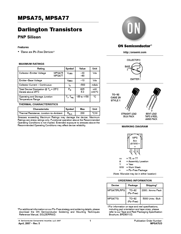
Package: TO-92-3
Mount Type: Through Hole
Pins: 3
Max Operating Temp: 150 °C
Key Features
- These are Pb--Free Devices*
| Part | MPSA75 |
|---|---|
| Description | PNP Transistors |
| Category | Transistor |
| Manufacturer | onsemi |
| Size | 136.32 KB |
Package: TO-92-3
Mount Type: Through Hole
Pins: 3
Max Operating Temp: 150 °C
| Seller | Inventory | Price Breaks | Buy |
|---|---|---|---|
| Win Source | 50000 | 420+ : 0.1379 USD 1025+ : 0.1132 USD 1580+ : 0.1097 USD 2180+ : 0.1062 USD |
View Offer |
| Worldway Electronics | 12272 | 7+ : 0.0271 USD 10+ : 0.0265 USD 100+ : 0.0257 USD 500+ : 0.0249 USD |
View Offer |
| Part Number | Manufacturer | Description |
|---|---|---|
| MPSA75 | Philips Semiconductors | PNP Transistor |
| MPSA75 | Central Semiconductor | SILICON PNP DARLINGTON TRANSISTORS |
| MPSA75 | Motorola Semiconductor | Transistors |
| MPSA70 | Central Semiconductor | PNP SILICON TRANSISTORS |
| MPSA76 | Central Semiconductor | SILICON PNP DARLINGTON TRANSISTORS |