MPSW13 Datasheet Text
MPSW13 One Watt Darlington Transistor
NPN Silicon
Features http://onsemi.
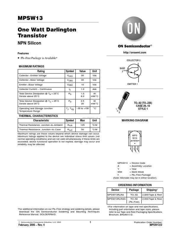
COLLECTOR 3 BASE 2
- Pb- Free Package is Available-
MAXIMUM RATINGS
Rating Collector
- Emitter Voltage Collector
- Base Voltage Emitter
- Base Voltage Collector Current
- Continuous Total Device Dissipation @ TA = 25°C Derate above 25°C Total Device Dissipation @ TC = 25°C Derate above 25°C Operating and Storage Junction Temperature Range Symbol VCES VCBO VEBO IC PD PD TJ, Tstg Value 30 30 10 1.0 1.0 8.0 2.5 20
- 55 to +150 Unit Vdc Vdc Vdc Adc W mW/°C W mW/°C °C 1 2
EMITTER 1
TO- 92 (TO- 226) CASE 29- 10 STYLE 1 3
THERMAL CHARACTERISTICS
Characteristic Thermal Resistance, Junction- to- Ambient Thermal Resistance, Junction- to- Case Symbol RqJA RqJC
..
Max 125 50
Unit °C/W °C/W
MARKING DIAGRAM
Maximum ratings are those values beyond which device damage can occur. Maximum ratings applied to the device are individual stress limit values (not normal operating conditions) and are not valid simultaneously. If these limits are exceeded, device functional operation is not implied, damage may occur and reliability may be affected.
MPS W13 AYWW G G
MPSW13 = Device Code A = Assembly Location Y = Year WW = Work Week G = Pb- Free Package (Note: Microdot may be in either location)
ORDERING INFORMATION
Device MPSW13RLRA MPSW13RLRAG Package TO- 92 TO- 92 (Pb- Free) Shipping † 2,000/Tape & Reel 2,000/Tape & Reel
- For additional information on our Pb- Free strategy and soldering details, please download the ON Semiconductor Soldering and Mounting Techniques Reference Manual, SOLDERRM/D.
© Semiconductor ponents Industries, LLC, 2006
†For information on tape and reel specifications, including part orientation and tape sizes, please refer to our Tape and Reel Packaging Specifications Brochure,...