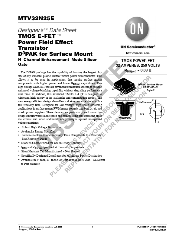
Datasheet4U Logo Datasheet4U.com

MTV32N25E - Power Field Effect Transistor

Key Features

  • power electronic loads are During the turn.
  • on and turn.
  • off delay times, gate current is inductive; the data in the figure is taken with a resistive load, not constant. The simplest calculation uses appropriate which approximates an optimally snubbed inductive load. values from the capacitance curves in a standard equation Power MOSFETs may be safely operated into an inductive for voltage change in an RC network. The equations are: load; however, snubbing reduces switching.

📥 Download Datasheet

Datasheet Details

Part number MTV32N25E
Manufacturer onsemi
File Size 274.65 KB
Description Power Field Effect Transistor
Datasheet download datasheet MTV32N25E Datasheet

Full PDF Text Transcription (Reference)

The following content is an automatically extracted verbatim text from the original manufacturer datasheet and is provided for reference purposes only.

View original datasheet text
MTV32N25E Designer’s™ Data Sheet TMOS E−FET.™ Power Field Effect Transistor D3PAK for Surface Mount N−Channel Enhancement−Mode Silicon Gate The D3PAK package has the capability of housing the largest chip size of any standard, plastic, surface mount power semiconductor. This allows it to be used in applications that require surface mount components with higher power and lower RDS(on) capabilities. This high voltage MOSFET uses an advanced termination scheme to provide enhanced voltage−blocking capability without degrading performance over time. In addition, this advanced TMOS E−FET is designed to withstand high energy in the avalanche and commutation modes. The new energy efficient design also offers a drain−to−source diode with a fast recovery time.