N04L63W2A
Key Features
- Single Wide Power Supply Range 2.3 to 3.6 Volts
- Very low standby current 4.0µA at 3.0V (Typical)
- Very low operating current 2.0mA at 3.0V and 1µs (Typical)
- Very low Page Mode operating current 0.8mA at 3.0V and 1µs (Typical)
- Simple memory control Dual Chip Enables (CE1 and CE2) Output Enable (OE) for memory expansion
- Low voltage data retention Vcc = 1.8V
- Very fast output enable access time 25ns OE access time
- Automatic power down to standby mode
- TTL compatible three-state output driver
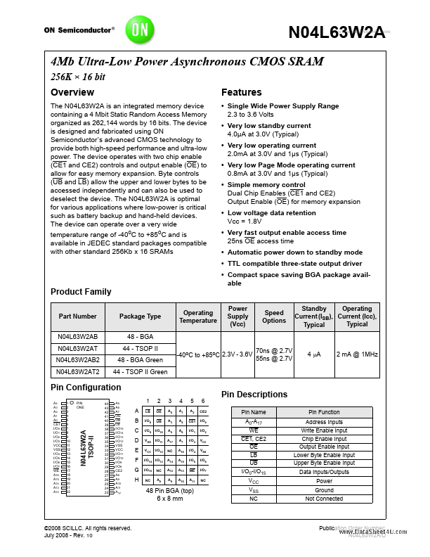
- Compact space saving BGA package available Product Family Part Number N04L63W2AB N04L63W2AT N04L63W2AB2 N04L63W2AT2 Package Type 48 - BGA 44 - TSOP II 48 - BGA Green 44 - TSOP II Green 70ns @ 2.7V -40oC to +85oC 2.3V - 3.6V 55ns @ 2.7V 4 µA 2 mA @ 1MHz Operating Temperature Power Supply (Vcc) Speed Options Standby Operating Current (ISB), Current (Icc), Typical Typical