Datasheet4U Logo Datasheet4U.com

NB3L553 - 2.5V / 3.3V / 5.0V 1:4 Clock Fanout Buffer

General Description

The NB3L553 is a low skew 1

clock distribution in mind.

to

output skew.

Optimal design, layout and processing minimize skew within a device and from device to device.

Key Features

  • Input/Output Clock Frequency up to 200 MHz.
  • Low Skew Outputs (35 ps), Typical.
  • RMS Phase Jitter (12 kHz.
  • 20 MHz): 29 fs (Typical).
  • Output goes to Three.
  • State Mode via OE.
  • Operating Range: VDD = 2.375 V to 5.25 V.
  • 5 V Tolerant Input Clock ICLK.
  • Ideal for Networking Clocks.
  • Packaged in 8.
  • pin SOIC.
  • Industrial Temperature Range.
  • These are Pb.
  • Free Devices Q1 Q2 ICLK Q3 Q4 OE Fig.

📥 Download Datasheet

Datasheet Details

Part number NB3L553
Manufacturer onsemi
File Size 273.40 KB
Description 2.5V / 3.3V / 5.0V 1:4 Clock Fanout Buffer
Datasheet download datasheet NB3L553 Datasheet

Full PDF Text Transcription (Reference)

The following content is an automatically extracted verbatim text from the original manufacturer datasheet and is provided for reference purposes only.

View original datasheet text
2.5 V / 3.3 V / 5.0 V 1:4 Clock Fanout Buffer
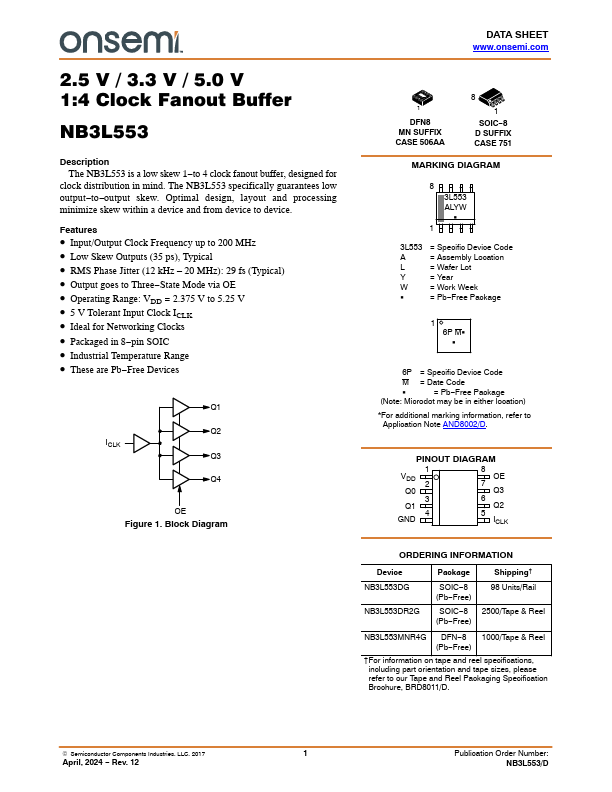
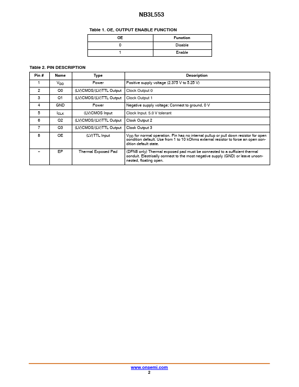
 NB3L553 Description The NB3L553 is a low skew 1−to 4 clock fanout buffer, designed for clock distribution in mind. The NB3L553 specifically guarantees low output−to−output skew. Optimal design, layout and processing minimize skew within a device and from device to device. Features • Input/Output Clock Frequency up to 200 MHz • Low Skew Outputs (35 ps), Typical • RMS Phase Jitter (12 kHz – 20 MHz): 29 fs (Typical) • Output goes to Three−State Mode via OE • Operating Range: VDD = 2.375 V to 5.25 V • 5 V Tolerant Input Clock ICLK • Ideal for Networking Clocks • Packaged in 8−pin SOIC • Industrial Temperature Range • These are Pb−Free Devices Q1 Q2 ICLK Q3 Q4 OE Figure 1. Block Diagram DATA SHEET www.onsemi.